半导体 (Semiconductor)
解决方案与软件
应用材料公司拥有广泛的能力和技术组合
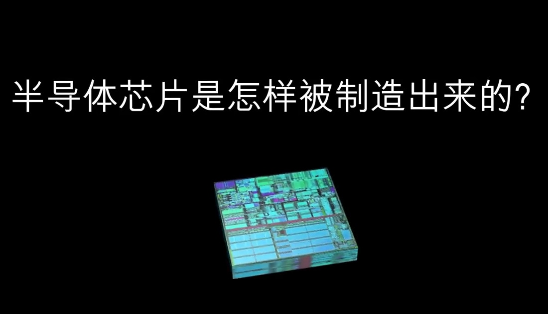
应用材料公司拥有业界广泛的互联半导体制造产品套件,专注于解决客户的高价值挑战并推动行业发展。我们的设备可以在晶圆表面沉积多层材料以改变材料的特性,以原子级精度塑造和移除材料,并分析材料和集成器件,用以加速功率、性能、面积、成本和上市时间。
半导体 (Semiconductor)
解决方案与软件
应用材料公司拥有业界广泛的互联半导体制造产品套件,专注于解决客户的高价值挑战并推动行业发展。我们的设备可以在晶圆表面沉积多层材料以改变材料的特性,以原子级精度塑造和移除材料,并分析材料和集成器件,用以加速功率、性能、面积、成本和上市时间。