半导体 (Semiconductor)
解决方案与软件
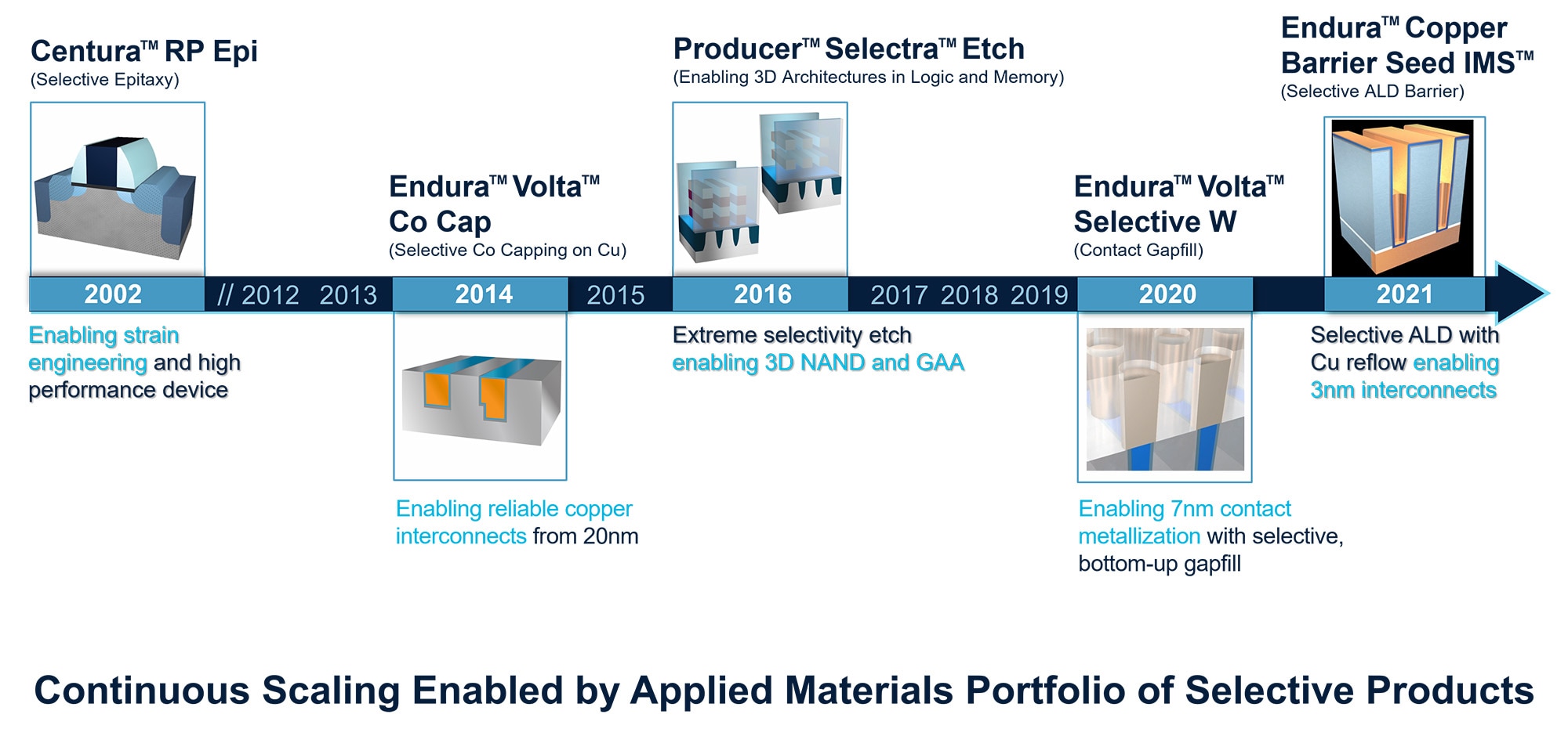
Selective Etch
Complex patterning schemes, higher aspect ratios, smaller vias and channels, more fragile features, and the increasing risk of pattern collapse are hastening the transition from bulk materials engineering to selective processing.techn
Selective processes use co-designed chemical and materials interactions to enable delicate and precise deposition and removal of target materials. Selective deposition and epitaxy is additive manufacturing at an atomic scale, putting atoms only where they are needed. Selective etch is subtractive manufacturing at an atomic scale, removing only unwanted atoms—even those beyond the line of sight—and leaving the rest in place. Selective deposition, epitaxy and etch technologies can be used to create and shape tiny patterns; fabricate novel structures; and overcome technology roadblocks such as the pattern collapse associated with wet processes, edge-placement errors in patterning, and 2D scaling issues associated with transistor contact and interconnect resistance.
Applied leads the industry in selective etch processes. The Producer Selectra Etch system removes dielectric, metal and semiconductor films with the atomic level precision required by today’s FinFET and GAA transistors structures.