Products & Technologies
Products & Services
Contact
Products & Services
Products & Technologies
Services
Resources
Contact
Media Kits
February 10, 2026 | Product Launch announced at SEMICON Korea 2026
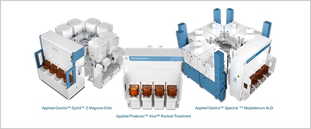
Applied Materials, Inc., the leader in materials engineering, today introduced new deposition, etch and materials modification systems that boost the performance of leading-edge logic chips at 2nm and beyond. The technologies supercharge AI compute through atomic-scale improvements to the most fundamental electronic building block – the transistor.
Media Briefing Presentations

October 7-9, 2025 | SEMICON West 2025
Applied Materials showcased breakthrough materials engineering technologies at SEMICON West, driving next-generation logic, memory and advanced packaging innovations essential for AI and high-performance computing. With industry-first solutions like Kinex™ hybrid bonding, Xtera™ epitaxial deposition, and PROVision™ eBeam metrology, Applied is accelerating chipmaker roadmaps to enable major device inflections and optimize performance, power, and cost.
Media Briefing Presentation Materials
Technology Breakfast
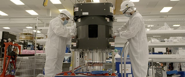
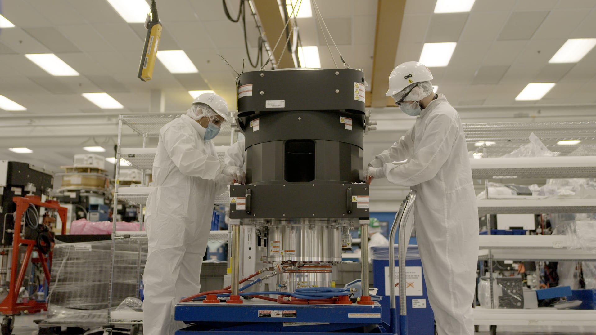
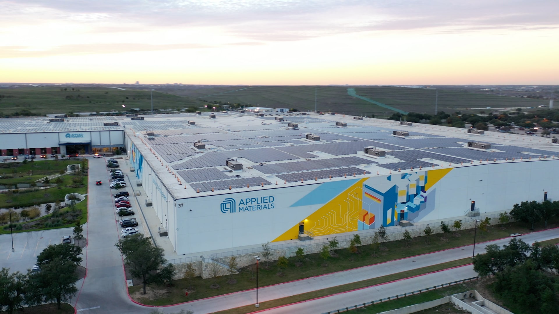
August 6, 2025 | U.S. Manufacturing Announcement
Applied Materials, Inc. is working with Apple and Texas Instruments (TI) to bolster the semiconductor manufacturing supply chain in the United States. Applied is supporting Apple’s partnership with TI, announced today, by supplying American-made chipmaking equipment from Austin, Texas to TI’s U.S. factories.

February 19, 2025 | SEMVision H20 Product Launch
Applied Materials, Inc. today introduced a new defect review system to help leading semiconductor manufacturers continue pushing the limits of chip scaling. The company’s SEMVision™ H20 system combines the industry’s most sensitive electron beam (eBeam) technology with advanced AI image recognition to enable better and faster analysis of buried nanoscale defects in the world’s most advanced chips.
System Renderings
SEMVision H20

November 21, 2024 | Applied Materials Breakthrough to Bring OLED Displays to Tablets, PCs and TVs
Applied Materials, Inc. today introduced the MAX OLED™ solution, a patented OLED pixel architecture and revolutionary display manufacturing technology designed to bring the superior OLED displays found in high-end smartphones to tablets, PCs and eventually TVs.

November 19, 2024 | Leadership Summit for Advanced Packaging
Applied Materials, Inc. today announced plans to expand its global EPIC* innovation platform with a new collaboration model specifically designed to accelerate commercialization of advanced chip packaging technologies.

July 9, 2024 | 2024 SEMICON West Technology Breakfast
Applied Materials, Inc. today introduced materials engineering innovations designed to increase the performance-per-watt of computer systems by enabling copper wiring to scale to the 2nm logic node and beyond. “The AI era needs more energy-efficient computing, and chip wiring and stacking are critical to performance and power consumption,” said Dr. Prabu Raja, President of the Semiconductor Products Group at Applied Materials.
Press Release
Applied Materials Unveils Chip Wiring Innovations for More Energy-Efficient Computing
Technology Breakfast
Presentation / Key Points
Video Animation
Endura™ Copper Barrier Seed IMS™ with Volta™ Ruthenium CVD
Profiles
Speaker Bios
Videos
We Work Here
How Do You Make a Semiconductor Chip
Supporting Our Communities
Our Newest Platform: Vistara
Pattern-Shaping Technology: Sculpta
Engineering the Gate-All-Around Transistor
Wiring Innovation: Endura CuBS Volta Ruthenium
Hybrid Bonding: Kinex
Selective Epitaxy: Xtera
B-roll
Applied Materials Corporate Headquarters
Semiconductor R&D and Manufacturing
Display Equipment
Brand Logos
Click logo to download
Visit our YouTube Channel for More Videos
Corporate Information

Contact Media Relations
Media and analyst inquiries, including requests for images and b-roll, can be directed to Media_Relations@amat.com