Products & Technologies
Products & Services
Contact
Products & Services
Products & Technologies
Services
Resources
Contact
Posted
January 23, 2026

Stay updated on our content.
Advancing Chip Performance with 30 Years of Wiring Leadership
by Zhebo Chen
AI models are outpacing Moore’s Law—and the wiring inside chips now determines how far we can push performance.
Across the entire wiring stack—from BEOL interconnects to the vertical links in advanced packaging—intricate networks move data and signals across billions of transistors. Since this wiring is as critical to system speed and efficiency as the compute cores themselves, unlocking its full potential demands a material that can deliver both high performance and scalability. For nearly three decades, copper has met a need with its outstanding conductivity, proven manufacturability, and compatibility with advanced architecture and packaging.
Scaling to Nanoscale Pushes Wiring to Its Limits
As AI’s relentless performance demands push chips to smaller nodes, wiring has scaled down in step with transistor advances. This extreme miniaturization means that in today’s AI processors, copper pathways stretch hundreds of miles across more than twenty layers, with some wires tens of thousands of times thinner than a human hair. At these dimensions, new hurdles emerge: resistance rises, reliability becomes harder to maintain, and barriers must strike a careful balance—thin enough to preserve space for copper yet strong enough to prevent failure.
These challenges have turned interconnects into a major performance bottleneck. And the constraints aren’t confined to the wafer: advanced packaging and 3D integration add another layer of interconnect complexity. With wiring now responsible for up to 80% of delay and power in advanced AI processors, even modest improvements can translate into significant throughput, latency, and overall performance gains—advances Applied Materials has been spearheading for decades.
From Barriers to Breakthroughs: 30 Years of Scaling Leadership
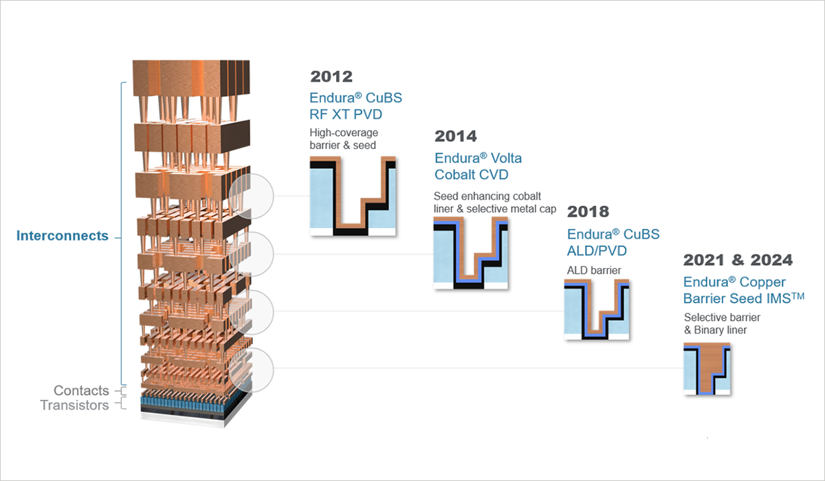
In 1997, Applied Materials launched the Endura™ Copper Barrier Seed (CuBS) system, combining liner and barrier deposition within ultra‑high‑vacuum to build robust copper interconnects. Since then, CuBS tools have advanced in a steady cadence of innovation to stay ahead of evolving architectural needs. Across multiple model iterations—Endura™ CuBS II (2004), CuBS RFX PVD (2009), and CuBS RF XT PVD (2012)—we refined physical vapor deposition to achieve thinner barriers and stronger seed continuity. These improvements boosted copper volume, reduced resistance, and ensured uniform layers for void‑free fill.
Continuing this momentum in materials and process co-optimization, we introduced the Endura™ Copper Barrier Seed IMS™ system in 2021. IMS combines multiple process families—such as physical vapor deposition, chemical vapor deposition and selective atomic layer deposition—within a single platform. Integrating these steps in vacuum preserves the integrity of deposited liners and barriers, which is critical for blocking electromigration and ensuring reliable copper fill. Building on that foundation, IMS incorporated a binary liner in 2024 that reclaimed more copper volume and reduced resistance for the smallest wires, while upper-level wires continue to leverage CuBS capabilities refined over previous generations.
Today, the Endura™ metallization platform sequences numerous tightly coupled vacuum steps, unifying complementary surface engineering, ALD, CVD, and PVD processes. This integrated materials solution delivers exceptional interconnect performance beyond 2nm and paves the way toward angstrom‑class manufacturing. For nearly thirty years, almost every copper chip produced worldwide has relied on an Endura™ system—a testament to its enduring role in shaping semiconductor technology.
Engineering Copper to Meet New Wiring Demands in Advanced Packaging
Applied Materials has pushed copper innovation not only in nanoscale BEOL wiring, but also across the rapidly evolving landscape of advanced packaging—where vertical connections and high‑density pathways demand equally powerful metallization solutions. Rising to the challenge of 3D wiring, we developed the Endura™ Ventura™ PVD system to enable through‑silicon vias (TSVs) at extreme aspect ratios.
By delivering uniform seed layers in structures up to ten times deeper than typical wiring, Ventura™ produced consistent deep-feature plating that reduced resistance and failure risk. This ultimately made TSV fabrication more cost-effective for scaling heterogeneous systems. As packaging complexity grew, Applied’s copper capabilities expanded to support fine-pitch and high-bandwidth features across stacked memory, interposers, and chiplets.
Copper Innovations Continue to Drive Next-Gen Systems
As transistor architectures move from planar to FinFET to gate‑all‑around and advanced packaging raises wiring demands, Applied’s copper innovations are key to delivering faster, more energy‑efficient systems. Still, performance isn’t driven by wiring alone. With contacts serving as the interface between the transistor and the wiring stack, contact-level advances amplify the benefits of advanced copper wiring.
Our recent post highlighted how Applied’s cutting-edge metrology validated molybdenum as a compelling low‑resistance contact option for advanced logic and memory. Stay tuned for our next blog, where we’ll explore how Applied is advancing contacts with innovative metal solutions, including molybdenum—bringing the same rigor in materials science and process integration to another critical layer of the stack.
Zhebo Chen
Global Product Manager, Atomic Layer Deposition (ALD) & Metal Deposition Products (MDP)

Zhebo Chen is the head of product management for the ALD & MDP business units at Applied Materials, supporting a wide spectrum of deposition technologies including ALD, CVD & PVD. Zhebo holds a bachelor’s degree in Chemical Engineering from the University of Illinois at Urbana-Champaign and a Ph.D. in Chemical Engineering from Stanford University.