Products & Technologies
Products & Services
Contact
Products & Services
Products & Technologies
Services
Resources
Contact
Posted
January 05, 2026

Stay updated on our content.
Co-optimized Process and Metrology Accelerates Molybdenum Contact Development

by Michael Shifrin, Max Gage and Zhebo Chen
As device scaling continues and connections to the transistors become even thinner, traditional tungsten (W) contacts face challenges in their ability to efficiently conduct electrons. Molybdenum (Mo or “Moly”), with its lower electrical resistivity at smaller dimensions, emerges as a promising alternative for next-generation contact applications in both logic and memory devices. Since contacts form the smallest connections between interconnects and transistors, maintaining low resistance is critical to ensure maximum device performance and efficient power consumption.
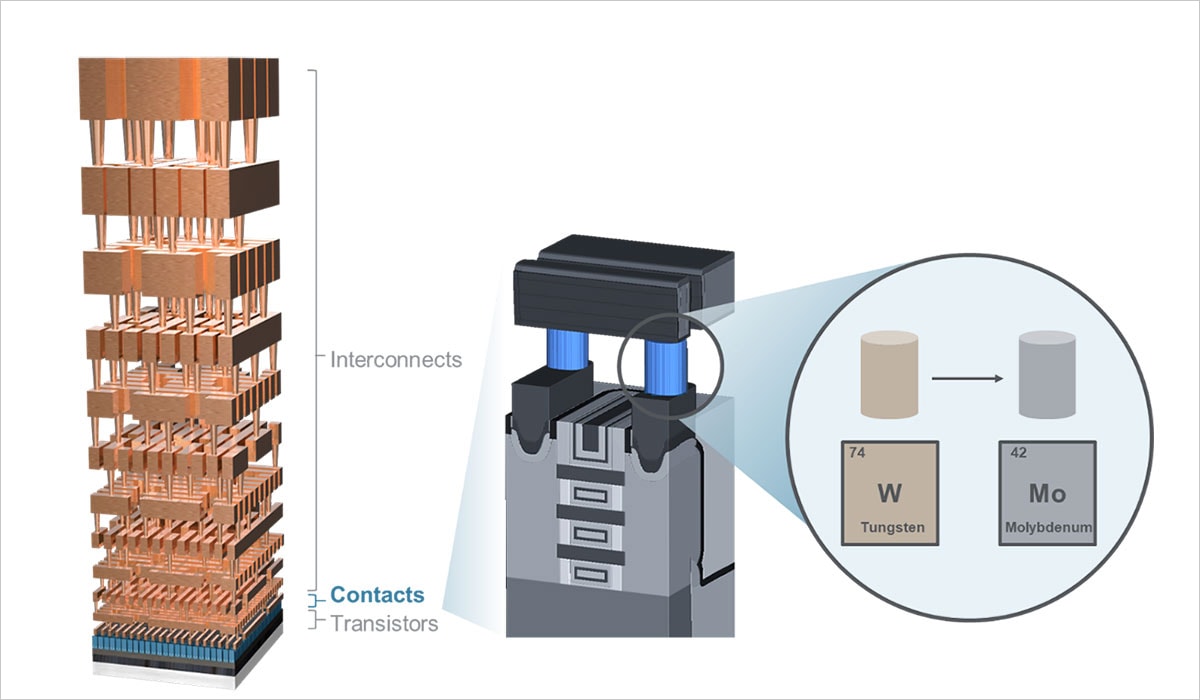
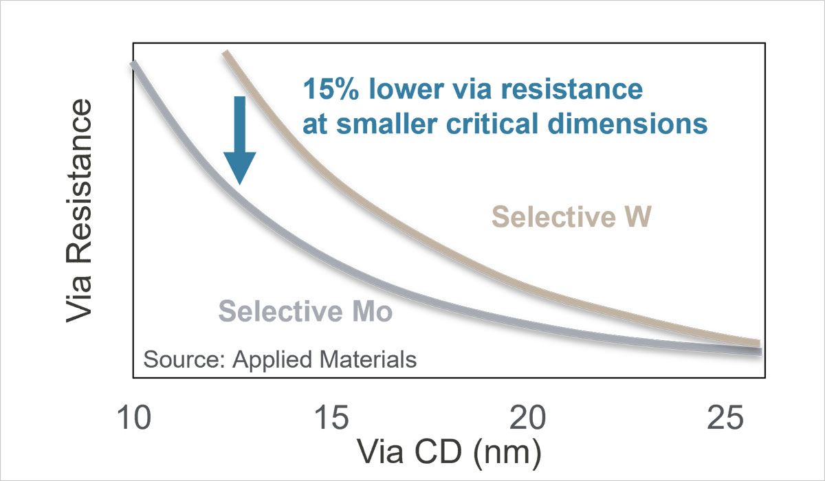
The industry’s gold standard has been Selective W, which lowers contact resistance by 40% compared to conventional W. Applied’s Selective Mo metallization technology can achieve an additional 15% lower resistance compared to Selective W in the tiniest features, supporting continued device scaling for gate-all-around transistors.
Novelty Often Comes with New and Unknown Challenges
To fully realize the benefits of lower resistivity, optimizing the Moly fill and planarization process is essential to meet strict specifications for material levels, uniformity, and planarization – all of which are critical to final device performance.
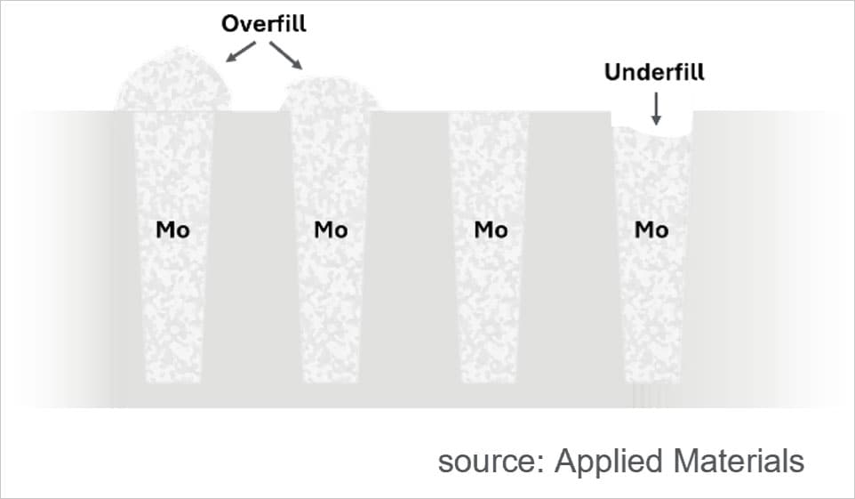
Deposition Challenges
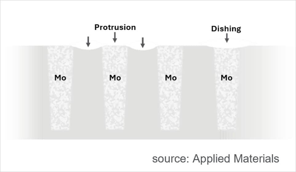
CMP Challenges
Traditionally, overfill, underfill, dishing, and protrusion measurements are obtained either through end-of-line testing or specialized lab analysis. However, both methods have significant drawbacks: they are often too slow, costly, or lack the detail needed to drive effective action. End-of-line tests occur late in the process and cannot pinpoint which specific steps caused a failure. While lab failure analysis can be tied to a particular process step, it is expensive, takes days to complete, and yields only a limited number of data points across the wafer.
One of the main challenges for process engineers is speeding up the optimization of process parameters, which often demands numerous experiments. Accurately characterizing process variations requires identifying signatures and trends across the wafer, necessitating large volumes of data from many “hot spots” – often extending an already lengthy diagnosis process. An effective metrology system should deliver rapid, ad-hoc insights by capturing tens of thousands of on-device samples across the wafer.
Co-optimized Processes and PROVision 10 Accelerate the Learning Curve
By combining Applied’s advanced eBeam process and metrology tools with the Maydan Technology Center’s rapid development environment, a novel Moly contact metrology system was created that leverages the Applied PROVision™ eBeam system. Close collaboration between the process and metrology teams enabled Applied to accelerate learning cycles, generating massive amounts of localized, on-device data in less than an hour with massive eBeam metrology.
During Applied Materials’ SEMICON West Technology Breakfast on October 7, 2025, Michael Chudzik, VP of Technology, outlined the importance of co-optimized technologies to accelerate research and development. Pairing processes with massive eBeam metrology dramatically compresses learning cycles.
Accelerated R&D capabilities facilitated the selection of Applied's Moly metallization tool by a leading advanced logic customer. The competition between Applied and its peers centered on closing the process loop efficiently and demonstrating stable recipe conditions that fulfilled all metallization requirements. By implementing the Moly contact metrology system developed at the Maydan Technology Center – leveraging PROVision 10’s advanced high-resolution eBeam imaging and shadow-based topography detection – the Applied teams were able to rapidly refine their recipes and earn the customer's confidence.
source: Applied Materials
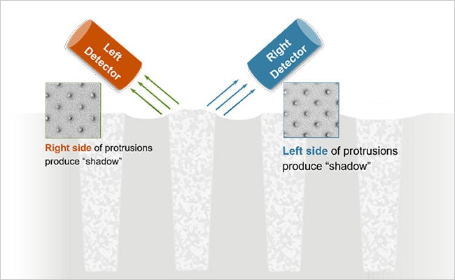
PROVision Protrusion Detection and Composite Imaging
The image above shows how PROVision 10 applies post-processing algorithms to topography data to identify dishing and protrusion after Moly CMP, aiding process engineers in visualizing and measuring layout density variations.
This functionality enabled the Applied team to:
- Visualize dishing, protrusion, and fill uniformity in relation to specific processes
- Rapidly identify process signatures across the wafer
- Shorten learning cycles
Applied’s Connectivity Strategy a Unique Value for the Industry
Technology development is becoming more complex as the industry advances toward smaller geometries and new 3D architectures. The interdependencies among processing steps have become increasingly important for achieving intended results. This case illustrates how integrating processes and capabilities can provide value that supports research and development efforts for customers.
Additionally, Applied is expanding its approach from connecting process capabilities to also facilitating connections between customers, partners, and the broader semiconductor ecosystem. This connectivity strategy is intended to help the industry collaborate on solving the most challenging problems.
Michael Shifrin
Director of Product Marketing, Patterning Control division

Michael Shifrin is Director of Product Marketing in the Patterning Control division at Applied Materials. He has over 20 years of experience in semiconductor metrology and process control, spanning both eBeam-based and optical techniques such as OCD. Prior to joining Applied, he held product marketing leadership roles at Nova and engineering leadership roles at Intel and Micron, with a focus on FEOL and BEOL process control across both logic and memory. Michael holds a master’s degree in Materials Nano-Science from Tel Aviv University and a bachelor's degree in mechanical engineering from Ben-Gurion University.
Max Gage
Director of Process Engineering, Chemical Mechanical Planarization (CMP) Group

Max Gage is a director of process engineering in the chemical mechanical planarization group at Applied Materials. He has over 17 years of experience in metals CMP process and product development, covering key inflections in new materials and device architectures. Max holds a bachelor’s degree in mechanical and aerospace engineering from Princeton University and a Ph.D. in materials science and engineering from Stanford University.
Zhebo Chen
Global Product Manager, Atomic Layer Deposition (ALD) & Metal Deposition Products (MDP)

Zhebo Chen is the head of product management for the ALD & MDP business units at Applied Materials, supporting a wide spectrum of deposition technologies including ALD, CVD & PVD. Zhebo holds a bachelor’s degree in Chemical Engineering from the University of Illinois at Urbana-Champaign and a Ph.D. in Chemical Engineering from Stanford University.