Products & Technologies
Products & Services
Contact
Products & Services
Products & Technologies
Services
Resources
Contact
Posted
September 16, 2025

Stay updated on our content.
Why the World Needs an Integrated Chiplet-to-Wafer Hybrid Bonder
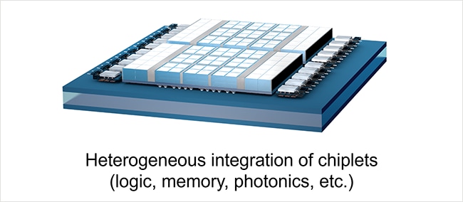
In response to escalating computation demand for artificial intelligence, the semiconductor industry has embraced heterogeneous integration technologies to develop advanced accelerators. These solutions consolidate CPU, GPU, memory, input/output, and power management functionalities within a single package. The process involves separating logic, memory, and other components into distinct dies or chiplets, which are subsequently assembled using high-density, low-latency, and low-resistance interconnects. This approach improves both electrical and thermal performance and contributes to reduced power consumption.
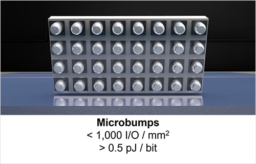
In common practice, chiplets are connected via microbumps, which consist of metal studs topped with solder balls. Chiplets equipped with microbumps are positioned together and heated in a reflow oven, melting the solder to establish interconnections; alternatively, thermal compression bonding may be used, applying pressure and heat to bond each chiplet. Microbump interconnects are typically arranged at a pitch between 25 and 50 microns, allowing for an interconnect density of several hundred per square millimeter. Optimizing bump design and bonding techniques can further increase this density to several thousand per square millimeter, which is significant for high-bandwidth communication between small devices.
Microbump limitations are influenced by physical and material constraints. Reducing bump size and increasing density are affected by solder connection effectiveness – excess solder may result in bridging or shorts between adjacent bumps, while insufficient solder can leave open connections. Reliability at smaller scales is impacted by the formation of copper post and solder intermetallic compounds, which have different thermo-mechanical properties that can cause cracking and mechanical failures.
Enter Hybrid Bonding
To avoid microbump limitations, the semiconductor industry has adopted hybrid bonding technology, enabling die-to-die interconnections at densities of 100,000 per square millimeter or higher. Hybrid bonding, originally developed for image sensors and memory, establishes two types of connections between die surfaces: dielectric-to-dielectric bonds and copper-to-copper bonds. This methodology eliminates the requirement for solder or intermediate materials that degrade thermal and electrical performance. The first significant use of hybrid bonding for high-performance compute devices was AMD’s Ryzen 7 series processors with 3D V-cache introduced in 2022, where an external memory cache was hybrid bonded to a logic CPU. Currently, commercial stand-alone bonders are in use at leading-edge logic foundries, but an integrated hybrid bonding system is desperately needed to match the pace of advancements in AI.
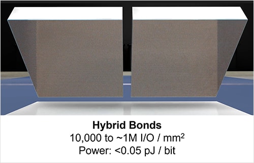
Hybrid bonding presents several key advantages. The absence of bumps and solder reduces bump pitch and helps to optimize vertical space utilization. The bond structure improves electrical performance by minimizing parasitic capacitance and resistance through direct connections, which in turn can enhance signal integrity, enable higher data transfer rates, and lower energy consumption. Compared to microbump techniques that use organic fillers with limited thermal conductivity, hybrid bonding promotes more effective heat dissipation and can result in lower junction temperatures during high-power operations, such as those in AI data centers, due to the exclusion of organic materials. Direct copper-to-copper connections may also address reliability concerns related to brittle intermetallic compound formation.
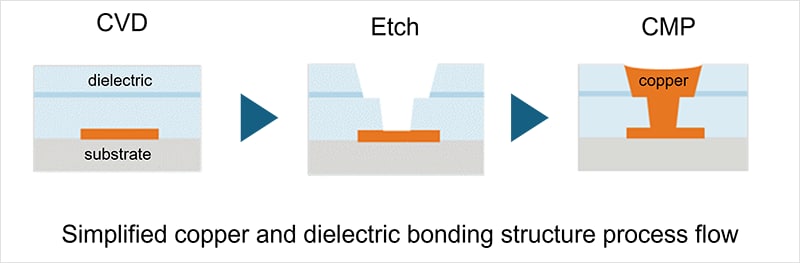
The hybrid bonding process involves creating copper and dielectric bonding structures on chiplets and target wafers intended for bonding. This is accomplished by using chemical vapor deposition (CVD) to deposit a silicon oxide or other dielectric layer that is later etched and filled with copper. Copper bonding pads are manufactured for external device connections, where chemical-mechanical polishing (CMP) achieves a smooth dielectric surface, with the copper pads recessed with nanometer-level precision below the surface. Maintaining consistent copper topography is important, as excessive recess can introduce interface voids and excessive protrusion may result in delamination.
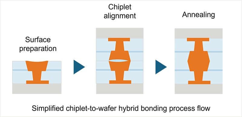
After forming copper and dielectric bonding structures, the singulated chiplets (on a wafer) are ready to be hybrid bonded to the target wafer containing the device substrate. First, the wafers are exposed to a low-energy plasma that activates the dielectric bonding film, followed by a water treatment that hydroxylates the wafer surfaces. Both wafers are subsequently moved to a hybrid bonder, where the chiplets are accurately aligned and placed in contact with the target wafer. The activated surfaces interact to create a temporary bond, which is then thermally annealed to produce a permanent dielectric-dielectric covalent bond. During thermal annealing, the copper pads expand and fuse, finalizing the hybrid bonding process.
The Need for Process Integration
The performance and reliability of hybrid bonding depend on several factors, including the chemical and physical properties of dielectrics and metals, surface conditions, and precise alignment. Since hybrid bonding requires direct dielectric-to-dielectric contact, any contamination – such as particles, residues, or edge defects from polishing and singulation – can compromise bond integrity. Additionally, the activated state of the bonding surface, induced by plasma and hydration treatments, degrades over time, reducing bonding energy and quality.
The challenges associated with the hybrid bonding process could be significantly reduced through the implementation of an integrated hybrid bonding system. Consolidating all key bonding capabilities – including the hybrid bonder, hydration, surface treatments and metrology – would enable precise control over the queue time between surface activation and bonding, ensuring consistency and minimizing variation. Additionally, such a solution could provide an isolated, clean, and controlled environment for wafer transport between processing steps, thereby reducing particle generation and surface contamination. Applied has been collaborating with Besi to jointly develop the industry’s leading integrated system, and we are looking forward to sharing more details about the progress we have made in the coming months. The semiconductor industry needs this integrated system to facilitate the bonding of more advanced chiplets and allow state-of-the-art AI accelerators to flourish.
Amulya Athayde
Senior Director of Strategic Marketing, Heterogeneous Integration Business Unit

Amulya Athayde is Senior Director of Strategic Marketing in the Heterogeneous Integration business unit at Applied Materials, responsible for product and business strategy. He has worked in the field of semiconductor fabrication since 1995 and has been involved in the development and commercialization of plasma etch, thermal deposition and wet clean process equipment. Amulya has a Ph.D. in chemical engineering from the University of Notre Dame and a Bachelor of Technology degree in chemical engineering from the Indian Institute of Technology, Bombay.