Products & Technologies
Products & Services
Contact
Products & Services
Products & Technologies
Services
Resources
Contact
Posted
July 16, 2025

Stay updated on our content.
Backside Power Demands Innovation in eBeam Metrology
In the race to deliver higher performance, lower power consumption and denser transistor arrays, semiconductor manufacturers are embracing a fundamental architectural shift known as the Backside Power Delivery Network (BSPDN). This technique moves power delivery from the traditional front side – already crowded with logic and signal routing – to the wafer’s backside, freeing up precious real estate for high-density transistor logic.
However, this revolutionary advancement introduces entirely new overlay and process control challenges that can significantly impact yield, cost and time-to-market if not properly addressed. At Applied Materials, we’re pioneering next-generation metrology solutions specifically designed to tackle these emerging hurdles by leveraging the advantages of the electron beam (ebeam).
Game-Changing Technology Brings New Metrology Challenges
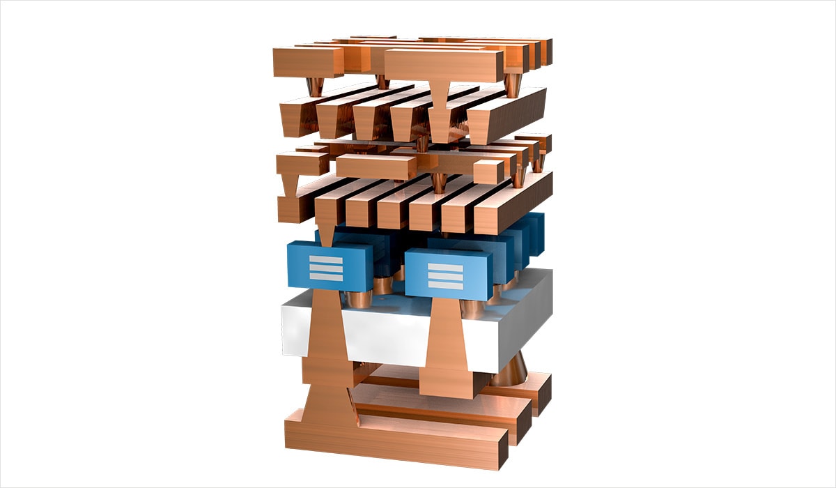
The backside power concept involves fabricating interconnects – known as backside vias – from the wafer’s backside, through the silicon substrate, and directly connecting to transistor-level structures such as the source/drain. The primary advantages are dramatically reduced resistance, shorter current paths and increased transistor density, all of which drives improved performance-per-watt for advanced logic, AI processors and next-generation mobile devices.
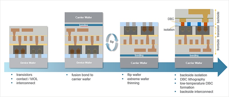
But integrating this novel architecture involves intricate wafer-bonding processes and additional high-precision manufacturing steps. Specifically, it requires bonding a carrier wafer to the front side, flipping the wafer, thinning it to sub-10-micron thicknesses, and then patterning and aligning backside contacts to previously fabricated front-side device layers. These additional wafer handling and bonding steps significantly amplify overlay complexity and introduce challenges, such as:
- Wafer distortion and stress induced by bonding, thinning and polishing steps
- Alignment difficulty due to hidden front-side reference layers obscured by backside processing
- Pattern-dependent wafer deformation, creating non-linear overlay errors difficult to predict and compensate
Without accurate overlay control, even the slightest nanoscale misalignments between backside vias and transistor-level structures can severely impact device performance, reliability and yield.
Traditional Overlay Methods Are No Longer Enough
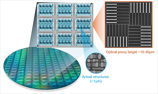
Historically, fabs have relied on optical overlay metrology using large proxy targets placed outside the active device area. But with backside power, these targets become less representative of actual device-level overlay. This disconnect grows even more severe as backside contacts land directly on tiny transistor-level features, such as the stacks of nanosheets that form the basis of the latest Gate-All-Around transistors. Simply put, traditional methods cannot reliably detect nanometer-level overlay errors that determine success or failure at the most advanced nodes.
The Need for Next-Generation eBeam Metrology
To navigate these unprecedented challenges, fabs urgently require unprecedented accuracy, resolution and efficiency in the measurement of direct backside contact overlay to capture the true device-level alignment between backside vias and nanosheets. Today’s Thermal Field Emission (TFE) tools will not be sufficient to enable high-volume production of chips with backside power and GAA transistor architectures. The industry needs a new generation of eBeam metrology to deliver a range of improvements:
- Higher resolution: Greater precision is required to accurately capture subtle overlay shifts and nanoscale misalignments, which is critical to controlling backside contacts that land on nanosheets or gate structures beneath complex stacks.
- Higher speed: The distortions and required corrections are of very high complexity – much beyond a basic offset or shift. These require more massive metrology, with 10-100x more measurements per wafer. Higher speed is critical because the metrology step cannot be prolonged.
- Higher landing energy: The next generation of metrology tools need to operate at high landing energies (up to 60 keV) to enable penetration deep into complex 3D stacks. This allows direct measurement of backside via placement relative to front-side transistor-level features without destructive cross-sectional analysis, which can directly improve yield in advanced backside power networks.
- More efficient collection of Back-Scattered Electrons (BSE): Advanced BSE detector technology can enable significantly enhanced collection efficiency, providing improved material contrast and clearer imaging of buried structures. High-quality BSE signals enable robust detection of subtle overlay misalignment in multi-layer, 3D integrated structures.
- Advanced algorithms for contour extraction: To complement the advanced imaging capabilities, next-generation tools need powerful algorithms for image enhancement, noise reduction and contour extraction. These sophisticated software tools enhance measurement accuracy while overcoming eBeam-induced charging challenges, allowing precise overlay measurements of backside contacts directly onto nanosheet structures – exactly where traditional optical tools struggle.
Addressing these challenges can allow chipmakers to directly measure overlay between backside contacts and transistor features, identify wafer-level distortion and stress-induced misalignment early in the fabrication process, and achieve tighter process control for backside via placement – all of which can significantly reduce overlay errors, resulting in a real-world impact on process yield. Applied is working with leading customers to develop new metrology systems that will address these challenges, helping customers to accelerate ramp and high-volume production of advanced backside power architectures, ensuring that their fabs stay ahead of the competition while addressing power consumption needs. Stay tuned for more details in the coming months.
Michael Shifrin
Director of Product Marketing, Patterning Control division

Michael Shifrin is Director of Product Marketing in the Patterning Control division at Applied Materials. He has over 20 years of experience in semiconductor metrology and process control, spanning both eBeam-based and optical techniques such as OCD. Prior to joining Applied, he held product marketing leadership roles at Nova and engineering leadership roles at Intel and Micron, with a focus on FEOL and BEOL process control across both logic and memory. Michael holds a master’s degree in Materials Nano-Science from Tel Aviv University and a bachelor's degree in mechanical engineering from Ben-Gurion University.