Products & Technologies
Products & Services
Contact
Products & Services
Products & Technologies
Services
Resources
Contact
Posted
September 29, 2025

Stay updated on our content.
HBM Memory Demands eBeam Metrology
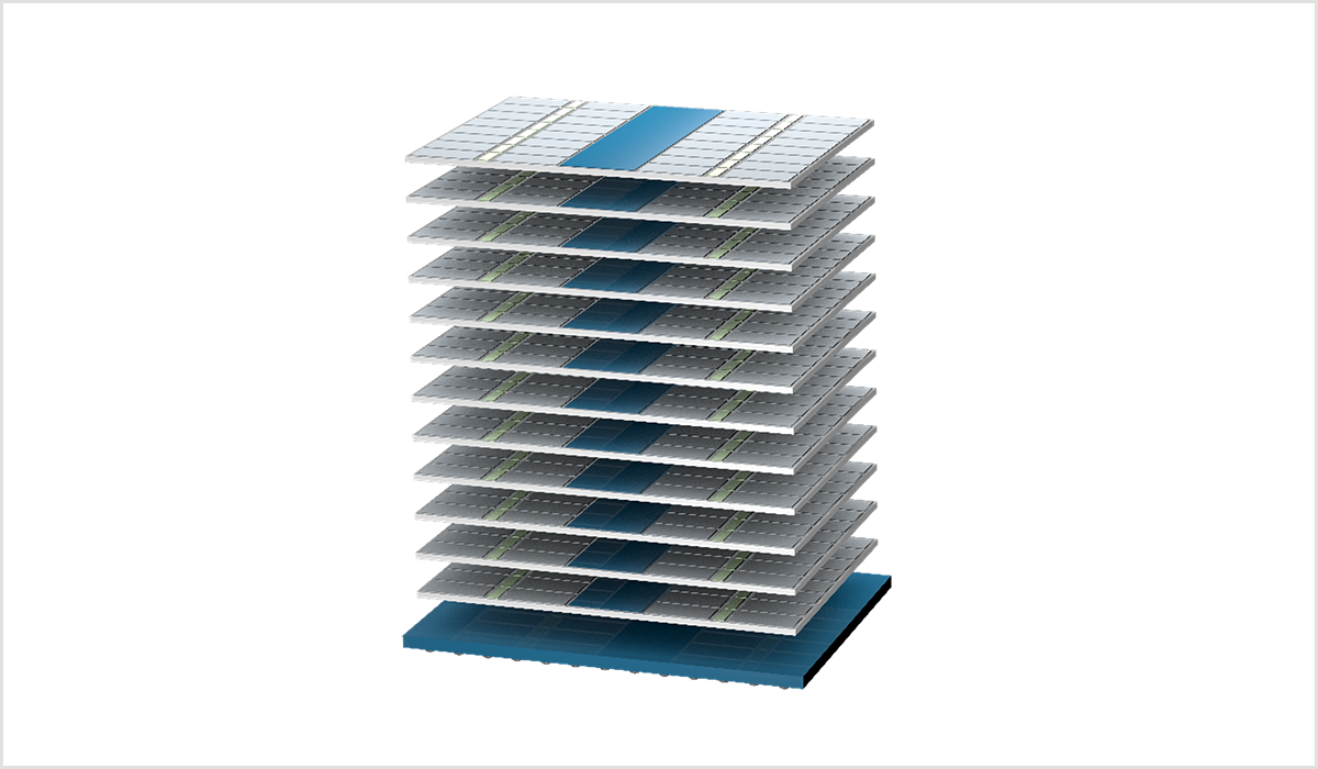
High Bandwidth Memory (HBM) is a 3D-stacked DRAM technology that provides unprecedented memory bandwidth by vertically integrating multiple DRAM dies, or chiplets. Modern AI accelerators (GPUs, AI processors, etc.) heavily rely on HBM because it delivers the highest memory data rates available – on the order of terabytes per second per stack. For example, HBM3E can achieve around 1.2 TB/s per stack, far outpacing conventional DDR or GDDR memory. This massive bandwidth is critical for feeding today’s AI models, whose sizes and dataset demands are growing exponentially (training model complexity has been increasing ~10x per year since 2012). Equally important, HBM’s architecture is power-efficient: by placing memory chiplets in close proximity to the compute chiplet (often on the same package or interposer), the data travel distance is minimized, reducing energy per bit. In short, HBM offers superior bandwidth and better energy efficiency, making it indispensable for AI, high-performance computing, and other data-intensive applications.
HBM’s performance comes with manufacturing challenges. Producing HBM stacks is far more complex than making traditional DRAM chips. Each HBM stack consists of multiple large DRAM chiplets (often 8–16 chiplets per stack) bonded to a base die. All must function perfectly in unison; if any chiplet in the stack is out of spec or defective, the entire HBM stack can fail. This drives an acute need for tight process control during fabrication – especially for critical dimensions (CDs) and pattern alignment – to ensure every die meets quality requirements before stacking. Conventional optical metrology struggles to help meet these requirements, which is why industry must now rely on advanced electron-beam (eBeam) metrology to address these challenges.
Why Precise Process Control is Critical for HBM Manufacturing
Large Chiplet Size & Limited Scribe Area:
HBM memory chiplets are physically much larger than standard DDR chips – in fact, a single HBM3E DRAM chiplet can be roughly twice the size of an equivalent-capacity DDR5 chip. These large chiplets occupy more wafer area, leaving less overall scribe area (the spacing between chiplets) for test structures.
Optical metrology traditionally relies on special targets in the scribe area to measure features like overlay error (misalignment between different patterned layers) and CD. With HBM’s chiplets using most of the reticle, there is less room for large optical targets. This forces more measurements to be made on the actual device. Optical tools struggle here because they require relatively large (often many microns wide), uniform targets and their pitch needs to be up to 10x larger than the device pitch, which introduces target-device errors. In contrast, eBeam metrology can directly image and measure features at the device level.
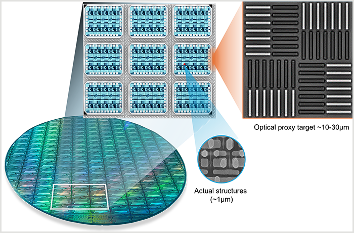
Optical metrology uses proxy targets to approximate measurements
In advanced memory fabs, scanning electron microscope (SEM) overlay measurements at final inspection have been used on device structures (post-etch) to complement optical data. The limitation of optical methods is evident from the difference between optical target measurements and on-chip reality. Studies have shown significant differences between development-inspection optical overlay versus SEM overlay on the actual patterns, often exceeding the tight overlay specs of about 2nm at the 1x nm node. Large HBM chiplets exacerbate this gap – thus more robust on-chip metrology (where optical is lagging) is needed to monitor and control HBM processes.
Stacked Chiplets Demand Minimum Variations in CD and Alignment
Unlike a single planar DRAM chip, an HBM stack’s performance and yield depend on every layer being in alignment and within tolerance. Variability in CD or misalignment (overlay error) on any chiplet can compound when chiplets are bonded together, potentially causing interface mismatches or timing errors in the HBM stack. Therefore, variability control for HBM must be extremely strict – far more critical than for stand-alone memory chips.
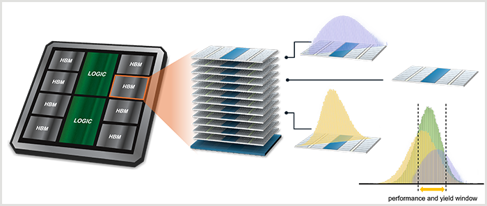
HBM variability, performance and yield determined by the whole stack
Memory manufacturers are now adopting eBeam metrology in high-volume production to tighten overlay and CD control. In advanced DRAM nodes (the same nodes powering HBM like “d1c” or “1α/1β”), SEM-based overlay measurements have already become an important supplement to optical methods. High-energy eBeam overlay metrology – using electrons with higher landing energy to penetrate and image multiple layers – allows direct measurement of overlay on actual device patterns, even for buried features that optical tools cannot see. This capability is crucial for HBM. Optical overlay targets, being placed in scribe lanes and not at device pitch, can only approximate the true overlay; they often cannot detect intra-chip overlay variation or pattern-dependent shifts.
eBeam, on the other hand, can measure overlay directly at the device level, yielding more accurate data to reduce variability across the wafer. Tight overlay control is paramount because HBM chiplets will later be vertically aligned; even a small layer-to-layer error can jeopardize TSV connections or cause cumulated edge placement error in the stack. By using on-chip eBeam metrology to catch overlay errors and CD variations, fabs can ensure each HBM chiplet stays within a narrow process window needed for stacking, ultimately improving stack yield and reliability.
Advanced Nodes (EUV Lithography) Shrink Error Budgets
The latest HBM generations (i.e., HBM3E and HBM4) are built on cutting-edge DRAM process nodes like d1c and d1d, which increasingly employ EUV lithography for critical layers. EUV introduces new challenges such as variability and stochastic defects – random pattern failures, line-edge roughness, and CD variation caused by photon shot noise and resist limitations. These stochastic defects eat into the allowable edge placement error (EPE) budget, leaving very little margin for overlay or CD errors before device performance is impacted. Essentially, at these nodes, the tolerance for any misplacement of edges (from all sources combined) is extremely tight.
Edge placement error
Conventional optical metrology is ill-equipped to monitor fine-grained stochastic variability across a chip, and this is where advanced eBeam metrology shines. Modern eBeam tools, especially those with Cold Field Emission (CFE) electron sources, offer sub-nanometer resolution imaging at high landing energies (up to ~50–60 keV) while maintaining high throughput. The high beam energy and improved electron optics allow eBeam systems to capture crisply defined contours of patterns and even probe through layers (via backscattered electrons) to measure cross-layer alignment in a way optical tools cannot.
As AI systems drive demand for these advanced HBM nodes, fabs are turning to multi-beam eBeam metrology tools that leverage parallel electron beams and CFE sources to achieve the required throughput (on the order of 5,000–10,000 measurement sites per hour) while still providing <1 nm measurement precision. Such tools enable massive data collection for stochastic defect analysis and EPE control.
HBM Needs Next-Generation eBeam Metrology
Deploying eBeam metrology with sub-nanometer resolution, high landing energy, and high throughput offers numerous benefits for HBM process control in advanced DRAM nodes. With the ability to measure extremely fine features and dense patterns across entire chiplets, eBeam systems enable engineers to monitor and optimize CD uniformity both locally and globally, detecting minute variations that optical tools might overlook. By precisely measuring edge placement error (EPE) on real device structures with direct edge detection and contour extraction, eBeam metrology identifies overlay shifts or line biases at the device level, reducing EPE variability and ensuring tighter layer alignment, which is essential for HBM’s rigorous performance and reliability demands.
Enhanced pattern fidelity is achieved as eBeam tools, especially those leveraging cold field emission sources, can accurately reconstruct the shapes and contours of features, enabling comparison to design intent and early detection of defects or distortions that could impact device consistency. Collectively, these advantages lead to higher yield and performance with lower power consumption, as process irregularities are caught and corrected at the nanometer scale, allowing more chiplets to meet specifications and improving the overall reliability and efficiency of HBM stacks. In the high-stakes environment of HBM manufacturing – where a single bad die can compromise an entire stack – tight process control through advanced eBeam metrology translates directly into better yield, reliable high-speed operation, and greater energy efficiency, all of which are crucial for the ever-growing demands of AI-driven systems.
eBeam metrology plays an important role in HBM technology, working alongside optical tools to achieve precision. With sub-nanometer resolution, high-energy electron optics for through-layer imaging, and improved throughput using multi-beam and CFE technologies, eBeam systems offer detailed insights needed to manage variability in advanced memory manufacturing. The use of eBeam metrology for HBM process control enables chipmakers to maintain strict fabrication tolerances across layers and chiplets in the stack. This supports AI accelerators by providing high-performance, low-power memory, along with yields suitable for large-scale production. In the context of rapid AI development, metrology-driven process control is essential for reliable manufacturing outcomes.
Michael Shifrin
Director of Product Marketing, Patterning Control division

Michael Shifrin is Director of Product Marketing in the Patterning Control division at Applied Materials. He has over 20 years of experience in semiconductor metrology and process control, spanning both eBeam-based and optical techniques such as OCD. Prior to joining Applied, he held product marketing leadership roles at Nova and engineering leadership roles at Intel and Micron, with a focus on FEOL and BEOL process control across both logic and memory. Michael holds a master’s degree in Materials Nano-Science from Tel Aviv University and a bachelor's degree in mechanical engineering from Ben-Gurion University.