Products & Technologies
Products & Services
Contact
Products & Services
Products & Technologies
Services
Resources
Contact
Posted
February 10, 2026

Stay updated on our content.
Powering the Next Era of Contact Scaling with ALD Molybdenum

By Zhebo Chen
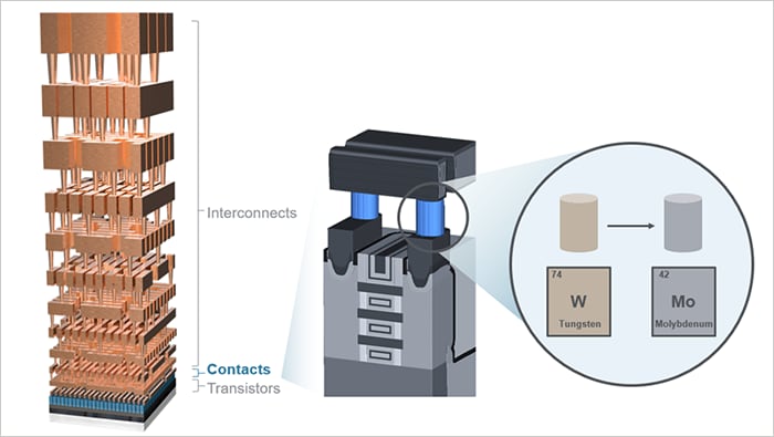
Imagine a race car trapped in bumper-to-bumper traffic. No matter how powerful the engine, that gridlock sets the pace. Inside today’s AI chips, the contact – the tiny metal bridge between each transistor and the wiring above – has become that traffic jam for electrons, dictating how fast signals can move.
Because every signal must pass through a contact first, this small structure has an outsized impact on performance and power efficiency. Choosing the right contact material – and perfecting how it’s deposited and integrated – has become essential to unlocking the next wave of gains as the industry advances beyond the 2nm era.
Tungsten’s Evolution: From Integrated Liner/Barrier to Selective W
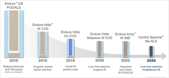
For many generations, chipmakers relied on tungsten as the primary contact metal. In 1998, Applied introduced the Endura™ Integrated Liner/Barrier (iLB) system, combining pre‑clean, physical vapor deposition (PVD), and chemical vapor deposition (CVD) in a single high‑vacuum platform to form low‑resistance tungsten contacts. Subsequently, the Endura iLB system added atomic layer deposition (ALD) for more uniform titanium nitride barrier coverage, extending tungsten’s viability at advanced nodes.
As the industry shifted to FinFETs, contact dimensions tightened dramatically. The barrier layer could not shrink proportionally, reducing conductive volume and driving resistance higher. Applied responded with materials innovations – thinner tungsten‑carbide liners and, in some structures, cobalt fill – to reclaim metal capacity and extend scaling.
Even so, a step‑change was needed as contacts approached the 7nm node. In 2020, Applied introduced the Endura™ Volta™ Selective W CVD system, combining specialized surface pre‑treatments with bottom‑up tungsten growth in a pristine vacuum. This allowed tungsten to be deposited directly on the transistor without a barrier, maximizing conductive metal fill. Consequently, early via deployments showed more than a 40% drop in contact resistance compared to conventional tungsten. The Endura™ Ioniq™ W IMS system further boosted performance by delivering high‑coverage tungsten PVD that enables chipmakers to form robust, pure‑metal tungsten contacts. This series of innovations solidified selective tungsten as the gold standard through the 2nm era.
A New Material Steps Up as Contact Scaling Stalls
Yet with escalating AI demand, the need to pack more transistors per area puts new pressure on the contacts. As devices shrink, contacts must shrink correspondingly, making this tiny structure one of the first places where scaling hits fundamental physical limits. In these ultra-narrow spaces, electrons collide with the sidewalls far more often, and this increased scattering escalates resistance sharply.
Applied recognized tungsten’s physics-driven limits early and prepared for what comes next – positioning molybdenum (moly) to carry contact scaling forward. Less sensitive to sidewall scattering, moly maintains lower resistivity as geometries tighten. In advanced test structures, Applied’s selective moly delivers ~15% lower contact resistance than selective tungsten. Scaled across billions of contacts, that reduction translates into meaningful system‑level speed and efficiency gains.
Breakthrough: Scaling Moly to HVM with Centris™ Spectral™ Mo ALD
While moly offers clear material advantages, achieving them demands an ultra‑clean interface, precise atomic alignment with the underlying lattice, and uninterrupted grain propagation across billions of features – each with different pattern densities, geometries, and surface conditions. These interdependent requirements have stalled industry progress for years.
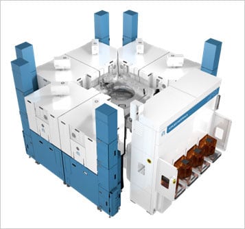
Solving issues of this complexity demands deep materials expertise – exactly where Applied shines. Enter the Spectral™ ALD system, one of the first in a new series of atomic layer deposition tools built on the proven Centris™ mainframe. Spectral™ ALD enables moly at scale, pairing specialized hardware with integrated process capability. Drawing on more than two decades of leadership in selective materials engineering, it delivers the atomic‑level control needed for bottom‑up, monocrystalline moly growth. Already shipped to multiple customers for advanced‑logic production, Spectral™ ALD provides fabs with a confident path to ramping moly contacts.
As AI workloads surge and nodes push deeper into the nanoscale, lowering contact resistance remains one of the most effective levers for improving speed and energy efficiency. By solving the materials and integration hurdles of selective moly, Applied is enabling the next generation of contact scaling – and accelerating the industry’s path into the angstrom era.
Zhebo Chen
Global Product Manager, Atomic Layer Deposition (ALD) & Metal Deposition Products (MDP)

Zhebo Chen is the head of product management for the ALD & MDP business units at Applied Materials, supporting a wide spectrum of deposition technologies including ALD, CVD & PVD. Zhebo holds a bachelor’s degree in Chemical Engineering from the University of Illinois at Urbana-Champaign and a Ph.D. in Chemical Engineering from Stanford University.