Products & Technologies
Products & Services
Company
Contact
Products & Services
Products & Technologies
Services
Resources
Company
Contact
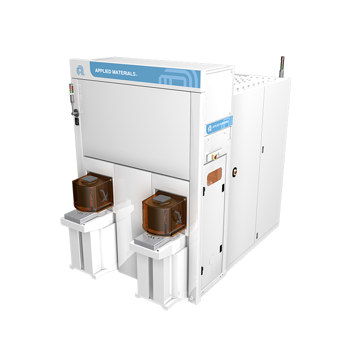
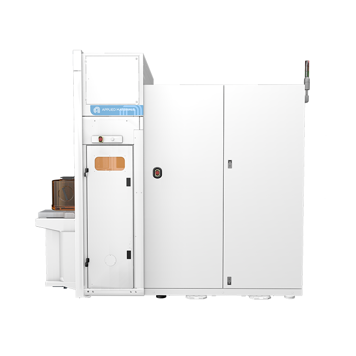
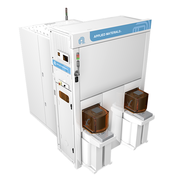
SEMVision G9 Defect Analysis
As semiconductor devices scale to smaller nodes and increasingly complex 3D architectures, fabs face mounting challenges in high‑volume manufacturing and growth across automotive, power, communication and IoT markets are pushing chip production to new levels. Additionally, high-density defect maps generated by optical inspection systems make it difficult for process engineers to quickly identify yield‑limiting defects and determine root cause. To maintain the tight process control required in high‑volume manufacturing, fabs need fast and more accurate defect review powered by high‑resolution imaging, real‑time classification, and actionable insight.
SEMVision® G9 addresses these challenges by delivering high‑throughput, high‑resolution automated defect review for a broad range of process layers and device types. Powered by Elluminator™ BSE see‑through imaging, e‑beam tilt, and high depth of focus, SEMVision G9 provides clear visibility into advanced high‑aspect‑ratio and 3D structures. Integrated, production‑proven deep‑learning capabilities – including ADR AI single‑image detection and Purity ADC AI classification – reduce nuisance defects, improve classification accuracy, and accelerate root‑cause analysis, enabling confident, real‑time manufacturing decisions while expanding review budget to more sites at speed.
SEMVision products have long set the industry standard for defect review, classification and analysis. SEMVision G9 is designed to operate alongside Applied’s cutting edge, 2nd generation cold field emission (CFE) platform, SEMVision H20, sharing AI resources, recipe flow, automation and a common user interface. Together, SEMVision G9 and H20 form a unified e‑beam ecosystem.
Learn More
- 1 / 3
- 2 / 3
- 3 / 3