Products & Technologies
Products & Services
Contact
Products & Services
Products & Technologies
Services
Resources
Contact

Stay updated on our content.
SEMVision™ G9 and the New Era of High-Volume Review
March 23, 2026
SEMVision G9 accelerates defect review across logic, memory and other devices, delivering higher productivity through trusted image quality and integrated AI that scales detection and classification across the fleet – at a competitive cost of ownership.
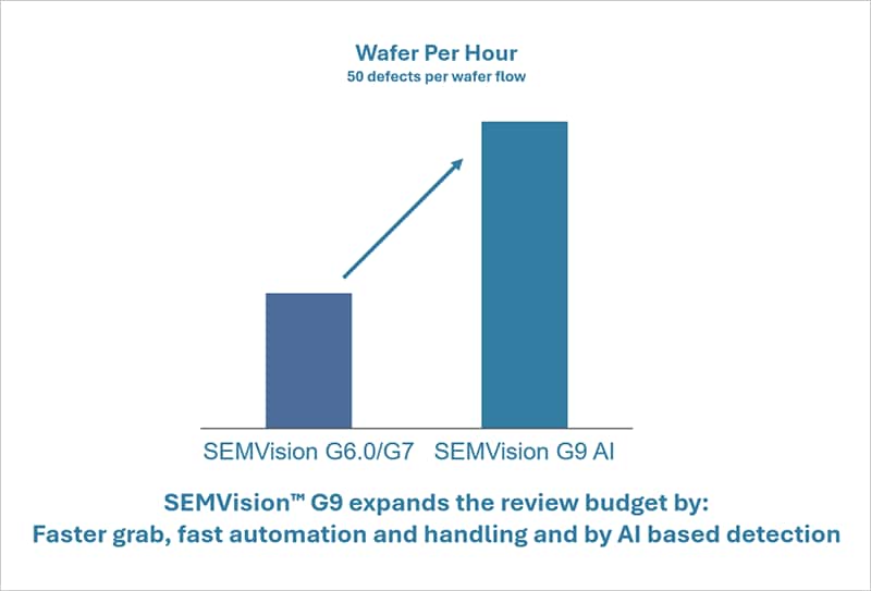
Why it matters: Increasing device complexity and 3D scaling are driving denser defect maps, creating load on review capacity SEMVision™ G9 expands the review budget by enabling more sites and samples at speed, so engineers can cover all layers - from FEOL to BEOL, without compromising cycle time or cost of ownership. Integrated AI further cuts manual effort and shortens time to result, accelerating high‑confidence production decisions.
What’s new:
- Improved imaging: higher beam current accelerates image acquisition, while increased maximum acceleration voltage paired with Elluminator™ wide back scattered electron (BSE) detector delivers clear visibility across challenging buried and high‑aspect‑ratio structures.
- Enhanced Image quality: Upgraded image‑processing algorithms provide best‑in‑class image quality, preserving defect signal even under noisy conditions
- Throughput & flow upgrades: Improved motion control and reduced overheads shorten end‑to‑end review time.
- Specialized AI flows: Mass-production‑proven ADR AI supports single image detection and CAD‑based detection, while ADC AI (Purity™ III) classification delivers faster, more accurate results.
- Continuity: plug-and-play support for world-leading SEMVision G7 recipes and imaging enables performance gains without disrupting production, with a full upgrade path from the SEMVision G7 family to the SEMVision G9.
Key applications: As the defect‑review leader, SEMVision supports a broad range of applications. The G9 brings unique capabilities, including beam e‑tilt, high depth-of-field-bevel imaging, DUV for bare and blanket wafers, material analysis, and the Elluminator wide BSE detector.
Bottom line: More wafers, more insight, less manual effort – SEMVision G9 pairs trusted imaging with integrated AI to drive faster, higher‑confidence production decisions.