Products & Technologies
Products & Services
Contact
Products & Services
Products & Technologies
Services
Resources
Contact
Centura iSprint SSW ALD/CVD
As semiconductor devices continue to scale to smaller dimensions and shift to new 3D structures, the challenge of metallizing contacts grows more complex. These contacts transport electrons from one location of the chip to another and are critical to device performance. For many years, conventional CVD tungsten was the process and material of choice to metallize many of these features due to its low resistivity and robustness against electro-migration. However, the evolution of features with higher aspect ratios or those that may have re-entrant overhang profiles can easily lead to seams and voids when filling with conventional CVD technology.
The Centura™ iSprint™ ALD/CVD Seam Suppressed Tungsten (SSW) system employs a treatment process that modulates the W growth at the locations of the feature where pinch-off may occur. This technology enables bottom-enhanced growth of tungsten metal. This unique deposition mechanism suppresses the formation of seams and voids which can be detrimental to resistance and yield. The versatility of the SSW system enables chip manufacturers to meet gapfill requirements for a wide variety of demanding features across multiple applications, including logic and memory, while simultaneously achieving high productivity in volume manufacturing.
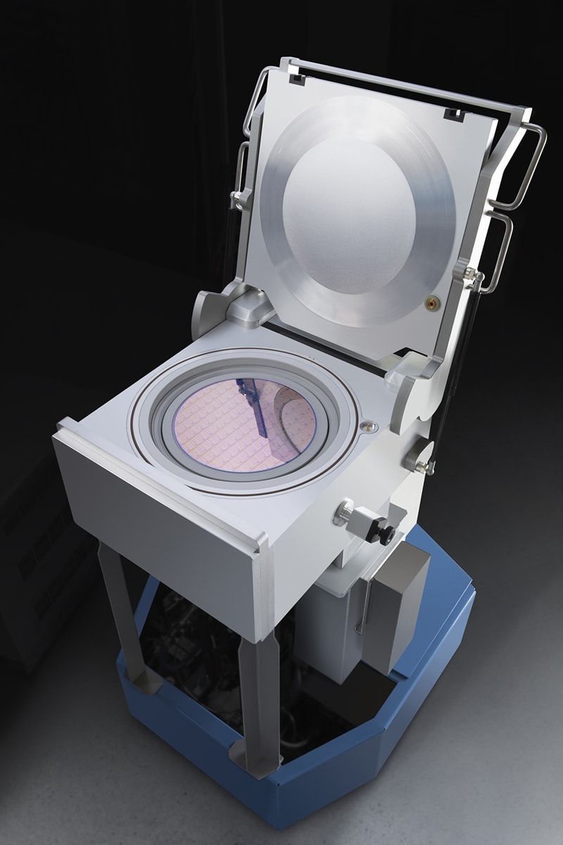
Employing a unique treatment process, the Centura™ iSprint™ SSW ALD/CVD process delivers a bottom-enhanced growth of tungsten metal that suppresses seams and voids, resulting in more robust gapfill and enhancing yield.