Products & Technologies
Products & Services
Contact
Products & Services
Products & Technologies
Services
Resources
Contact
Trending
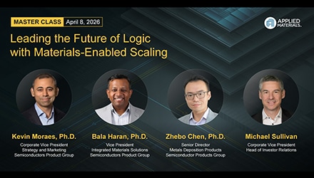
The Angstrom Era Explained: New Master Class Series Kicks Off April 8
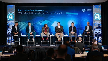
Applied Materials Convenes Industry Leaders on Advanced Patterning for the AI Era
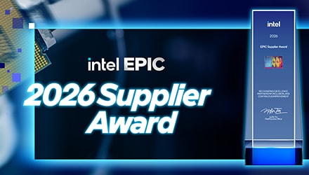
Applied Materials Receives Intel EPIC Supplier Award
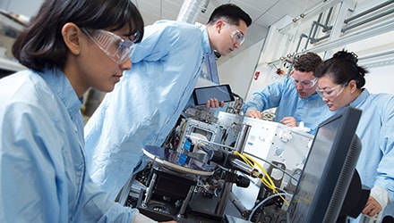
Applied Materials Accelerates Materials Simulation for the AI Era in Collaboration with NVIDIA