製品・サービス
製品・サービス
トレンド
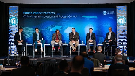
Applied Materials Convenes Industry Leaders on Advanced Patterning for the AI Era
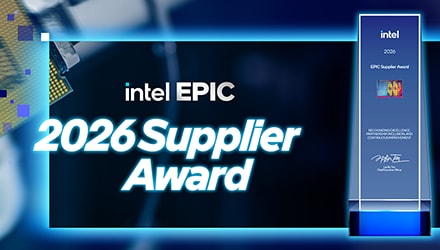
Applied Materials Receives Intel EPIC Supplier Award
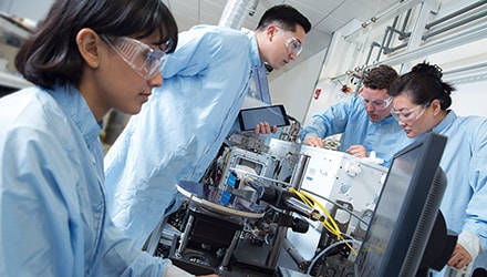
Applied Materials Accelerates Materials Simulation for the AI Era in Collaboration with NVIDIA

Applied Materials Raises Quarterly Cash Dividend by 15 Percent