半導體 (Semiconductor)
解決方案與軟體
DRAM 剖析
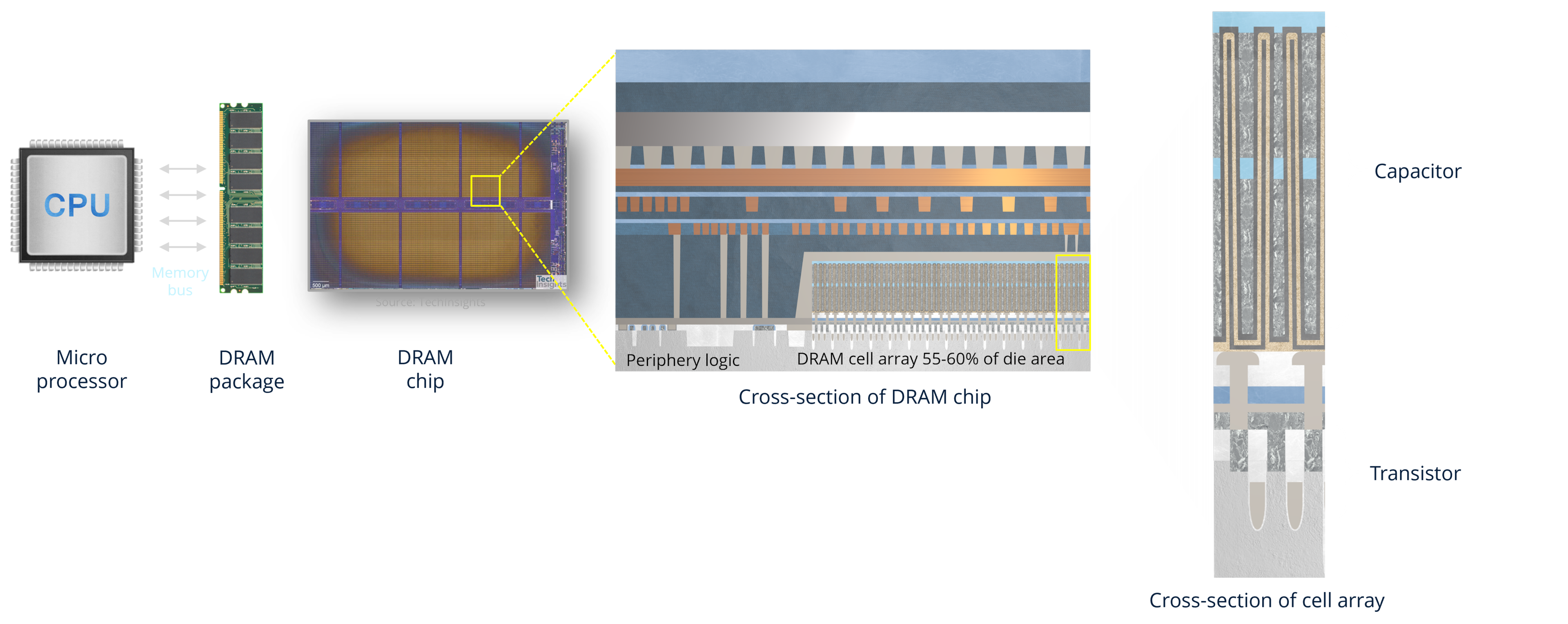
動態隨機存取記憶體 (DRAM) 是一種電腦元件,處理器可以在其中快速儲存每秒執行數十億次運算所需的資訊。典型的 DRAM 晶片有三個主要區域:
- 單元陣列,其中各個位元儲存在微型電容器中;
- 邏輯或核心區域,其中讀出放大器和字線解碼器等設備可幫助確定如何從單元陣列存取資料;
- 外圍設備,形成 DRAM 晶片內外的通訊鏈路。
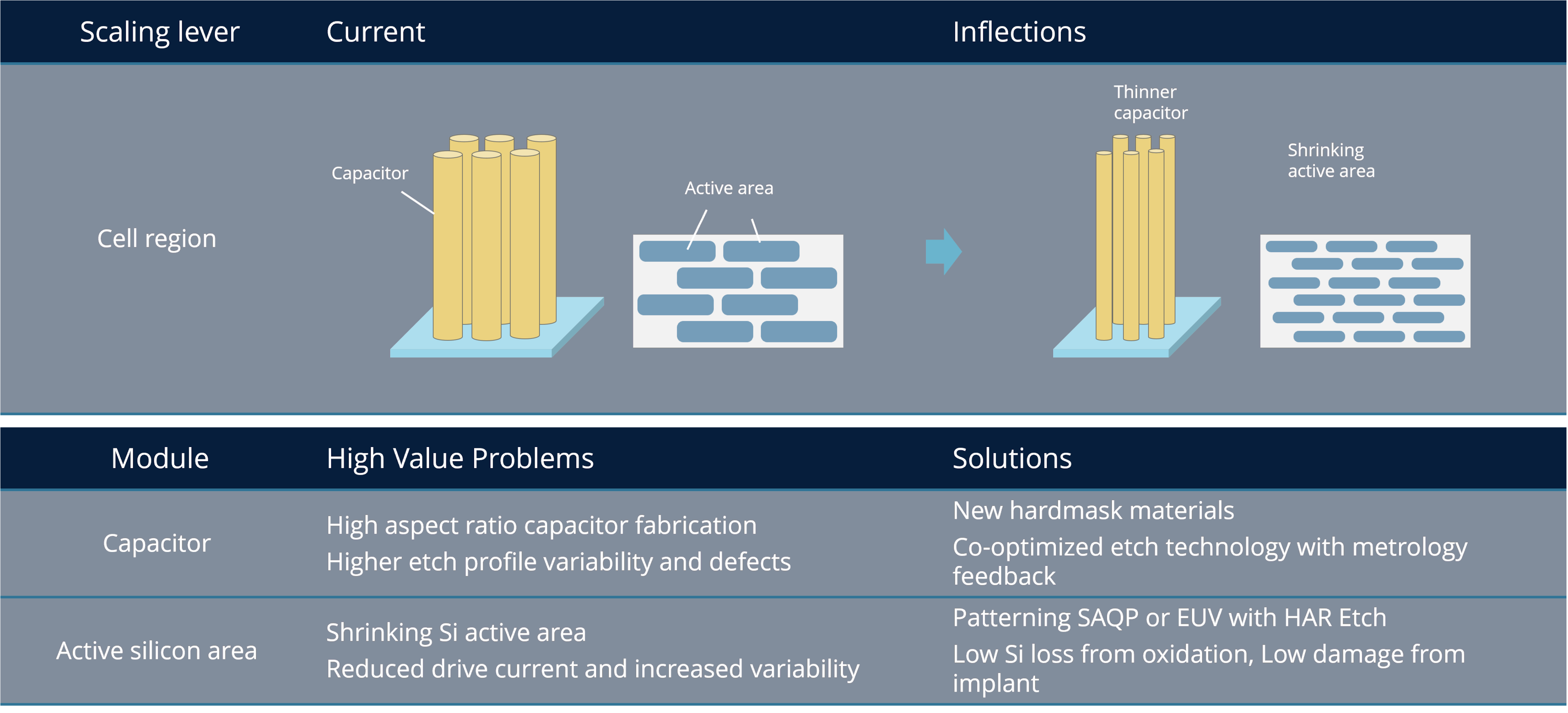
這三個區域都必須進行微縮,以滿足對於 DRAM 效能不斷增長的業界需求。這些微縮需求包括最大化可儲存在電容器中的電荷、減少讀出放大器的可變性以及減少因電路中的接線而導致的功率損耗。
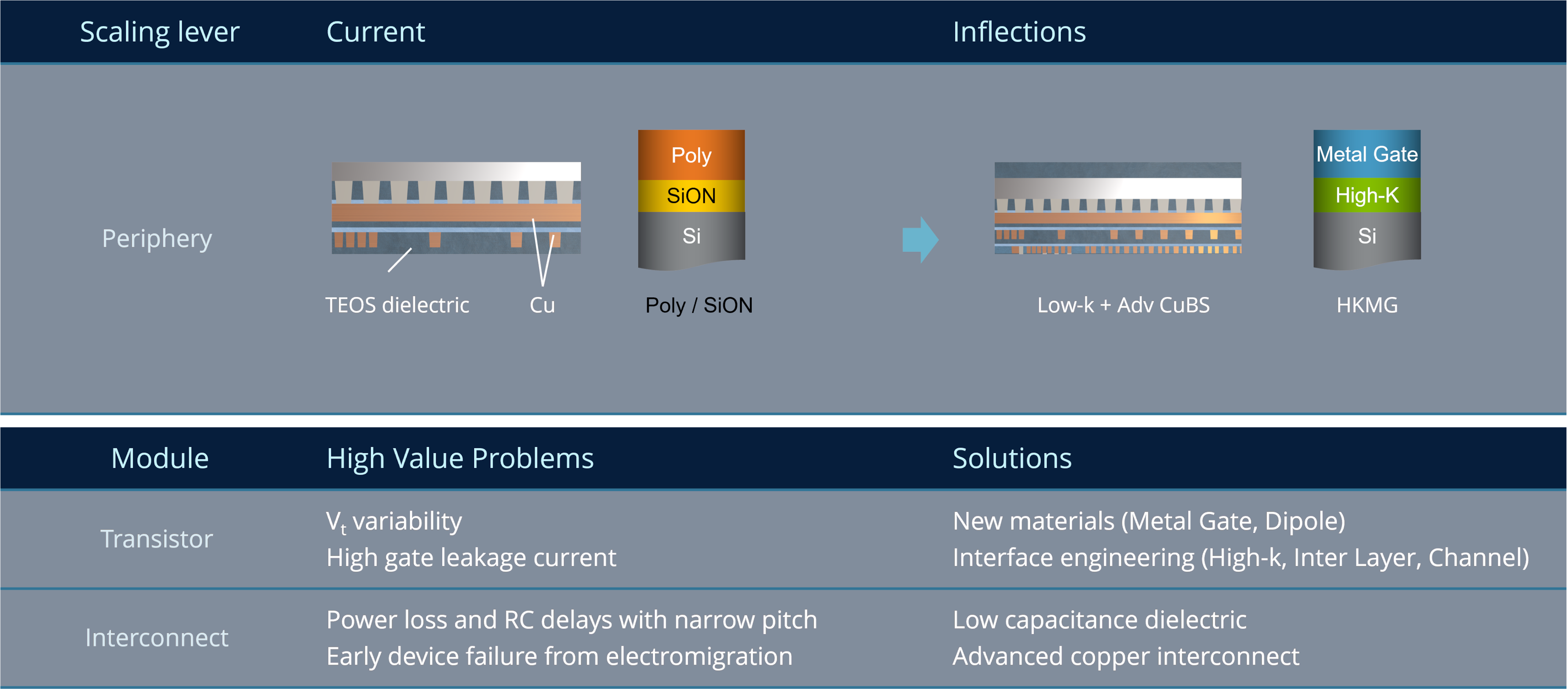
外圍邏輯微縮
DRAM 單元中的資料由外圍邏輯元件管理。外圍電路主要由高速邏輯電晶體和連接 DRAM 各部分的佈線組成。最大化該電路的訊號對於保持 DRAM 單元中儲存資訊的完整性至關重要。
許多 DRAM 製造商一直在用高介電值材料取代多晶矽介電質,用金屬閘極取代多晶矽閘極,以提高電晶體效能。 當多個不同的薄膜相互堆疊沉積時,任何出現在薄膜中或者介面上的缺陷皆會對電子傳輸造成重大的影響。
應用材料公司提供業界領先的低介電值產品Black Diamond,™用於 DRAM 後端銅佈線,以有效解決外圍邏輯區域尺寸微縮的需求。Black Diamond 的介電常數可降低 25%。 透過採用我們的Endura CuBS(銅阻障層/晶種)產品以及CVD 鈷,後端銅金屬化的可靠性提高了 10 倍以上。使用鈷封蓋有助於減少較高電流密度下的銅電遷移。
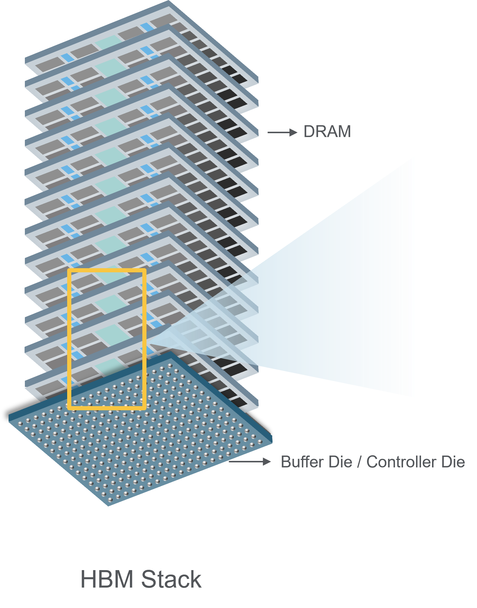
DRAM 堆疊 – HBM
為了提供人工智慧應用所需的大量記憶體,晶片製造商已轉向高頻寬記憶體 (HBM)——一種由先進DRAM堆疊構建的高效能、低延遲架構。雖然 DRAM 晶片的創新很重要,但 HBM的高密度和高頻寬其實是透過先進的 3D 封裝實現的。應用材料公司是材料工程領域的領導者,為HBM成長需求提供了所需的技術支援。 瞭解更多
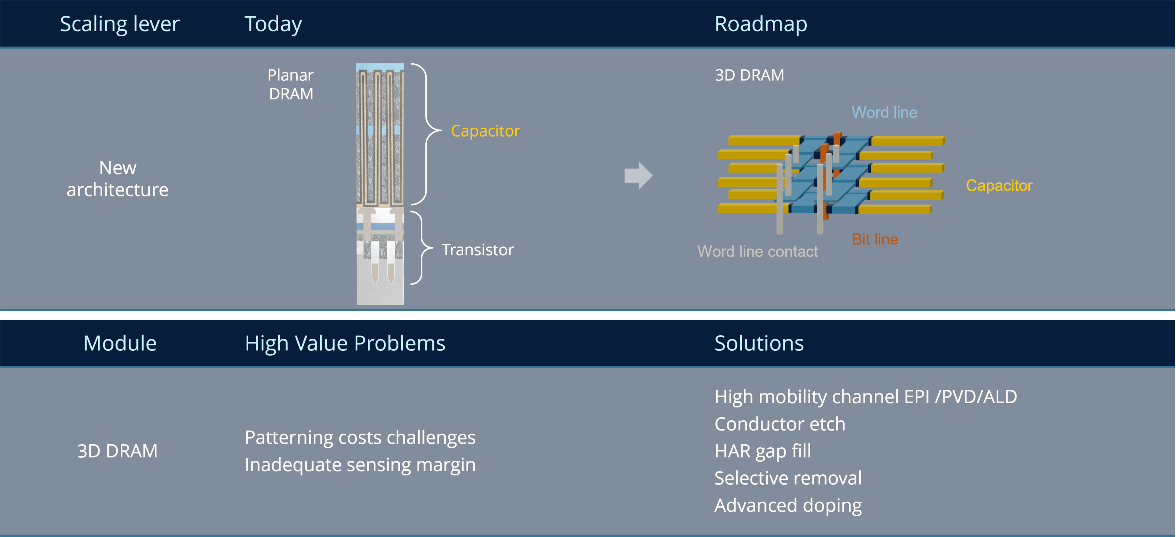
垂直微縮-3D DRAM
3D DRAM 是指在垂直方向上的位元架構儲存,類似於3D NAND。然而,DRAM 的速度幾乎比 NAND 快了近 1000 倍,這是因為 DRAM 使用高電子遷移率的矽基板作為起始材料來形成通道。DRAM的高速度也來自於電荷可以快速移入和移出電容器。 隨著 DRAM 在垂直方向上的擴展,需要新的材料創新來實現高遷移率和超低缺陷通道。
應用材料公司是新材料創新的領導者,這些技術可透過相關產品提供高電子遷移率材料,例如磊晶成長、PVD 和 ALD 等領域。沉積後,這些薄膜將被蝕刻以接觸底層。3D DRAM 預期需要先進的間隙填充、選擇性去除和先進的摻雜能力。這些能力必須無縫整合,以實現成功的解決方案。我們在開發整合性材料解決方案(Integrated Materials Solutions™) 方面的領先地位,將是共同最佳化不同製程的關鍵推動力,也將提供整體解決方案,以支持應對3D DRAM即將面臨的各種挑戰。