半導體 (Semiconductor)
解決方案與軟體
三維 NAND 解析
三維 NAND 也稱之為垂直 NAND (V-NAND),是一種非揮發性的快閃記憶體,其中儲存單元為垂直堆疊以增加儲存密度。 現今的三維 NAND 晶粒大約尺寸為 12mm x 6mm,具體大小取決於其密度。 傳統的三維 NAND 架構具有一組帶有階梯的單元陣列,旁邊有外圍電晶體。
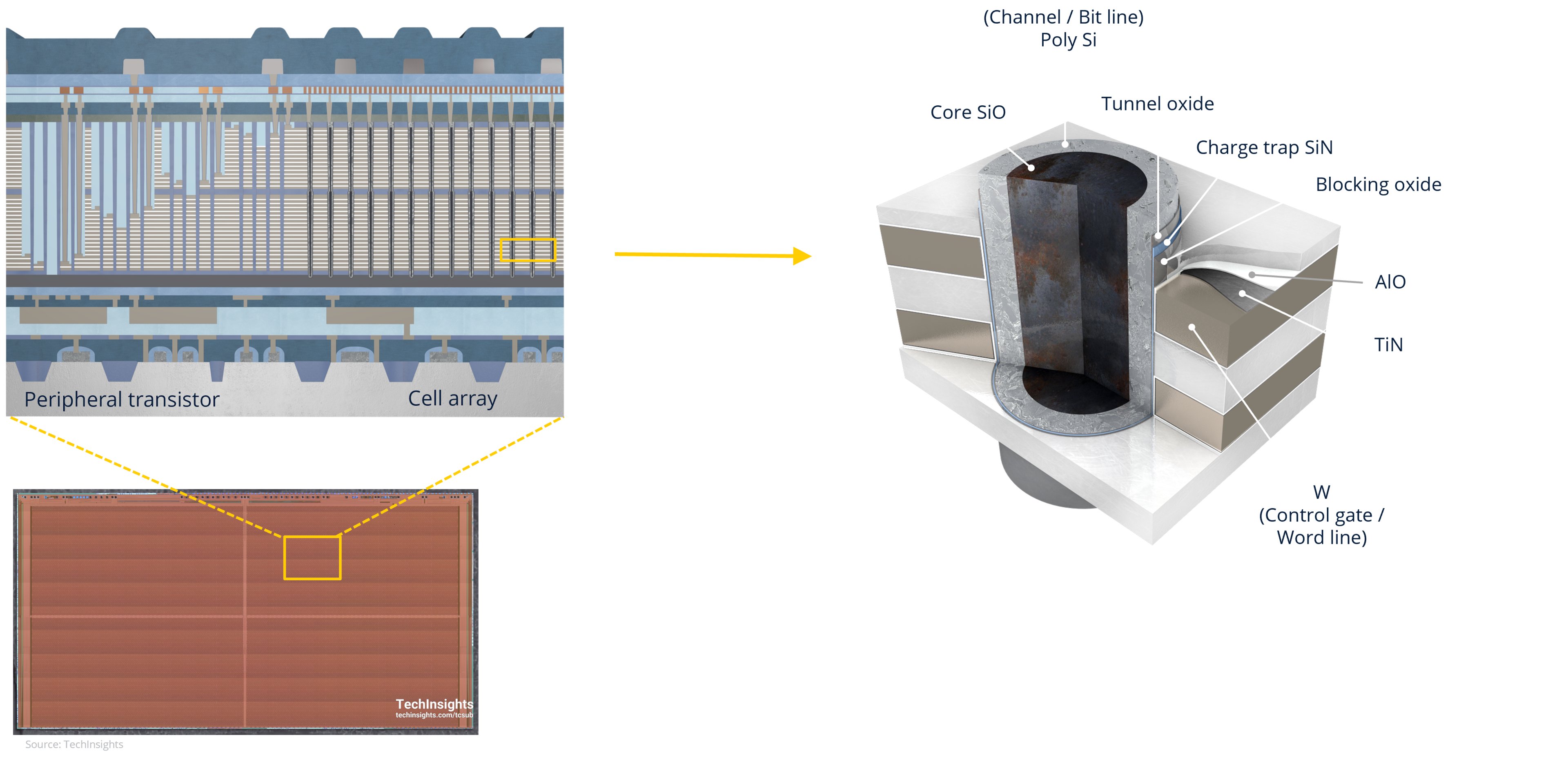
一個三維 NAND 儲存單元包含多個元件:
- W/TiN(鎢/氮化鈦)閘極
- AlO (氧化鋁)和阻擋氧化層,可控制能隙並阻止電子運動
- 矽氮化物捕捉層,可以儲存電子
- 穿隧氧化層
- 位於中心的多晶矽通道,用於在記憶體單元串列之間建立電氣連接
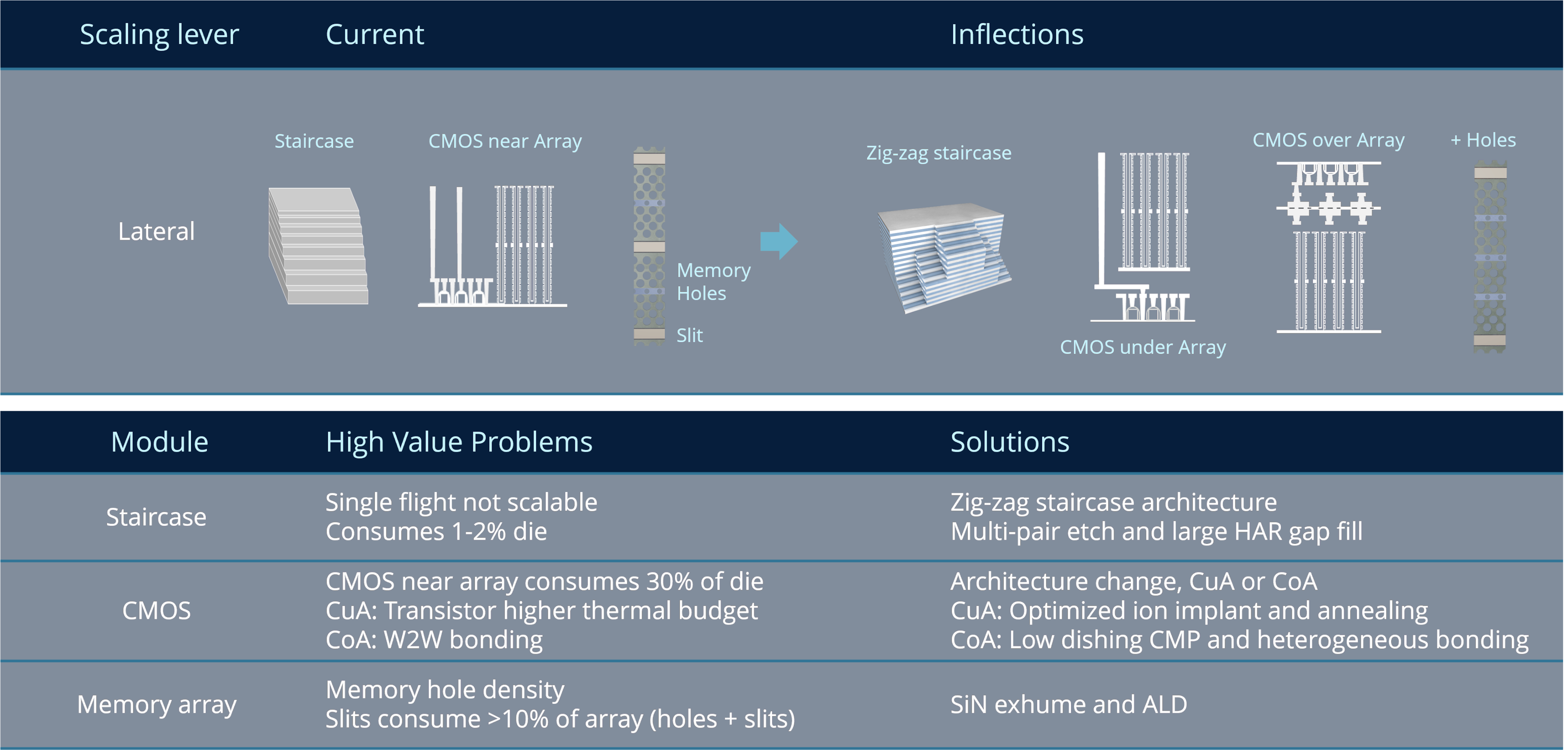
橫向微縮
橫向縮放需要減少階梯面積、外圍電路面積和狹縫面積。階梯的作用是充當柵極電極接觸的焊盤。透過在寬度方向而不是長度方向放置更多觸點,製造商可以節省整體樓梯長度。這種鋸齒形階梯結構帶來了挑戰,例如需要透過輪廓控制進行更深的蝕刻,以及保持臨界尺寸 (CD) 和蝕刻速率的均勻性。如今,記憶體製造商優先考慮這些類型的階梯式創新,而應用材料公司的Sym3已用於此目的,繼續保持我們在階梯式蝕刻領域的領先地位。
另外,也有可能在外圍的 CMOS 區域進行橫向微縮。 製造商正在將外圍電晶體移至記憶體陣列下方或上方,目標是節省約 10-15% 的晶片面積。 陣列下 CMOS (CuA) 的主要優點是其製造成本和良率損失較低。 然而,在 CuA 中的 CMOS 接面結構必須在單元形成之前製造。 與 CuA 相比,CMOS over Array (CoA) 中的 CMOS 電晶體必須在單獨的矽晶圓上製造。 在此之後,兩個晶圓必須進行鍵結以連接關鍵的金屬連接墊。
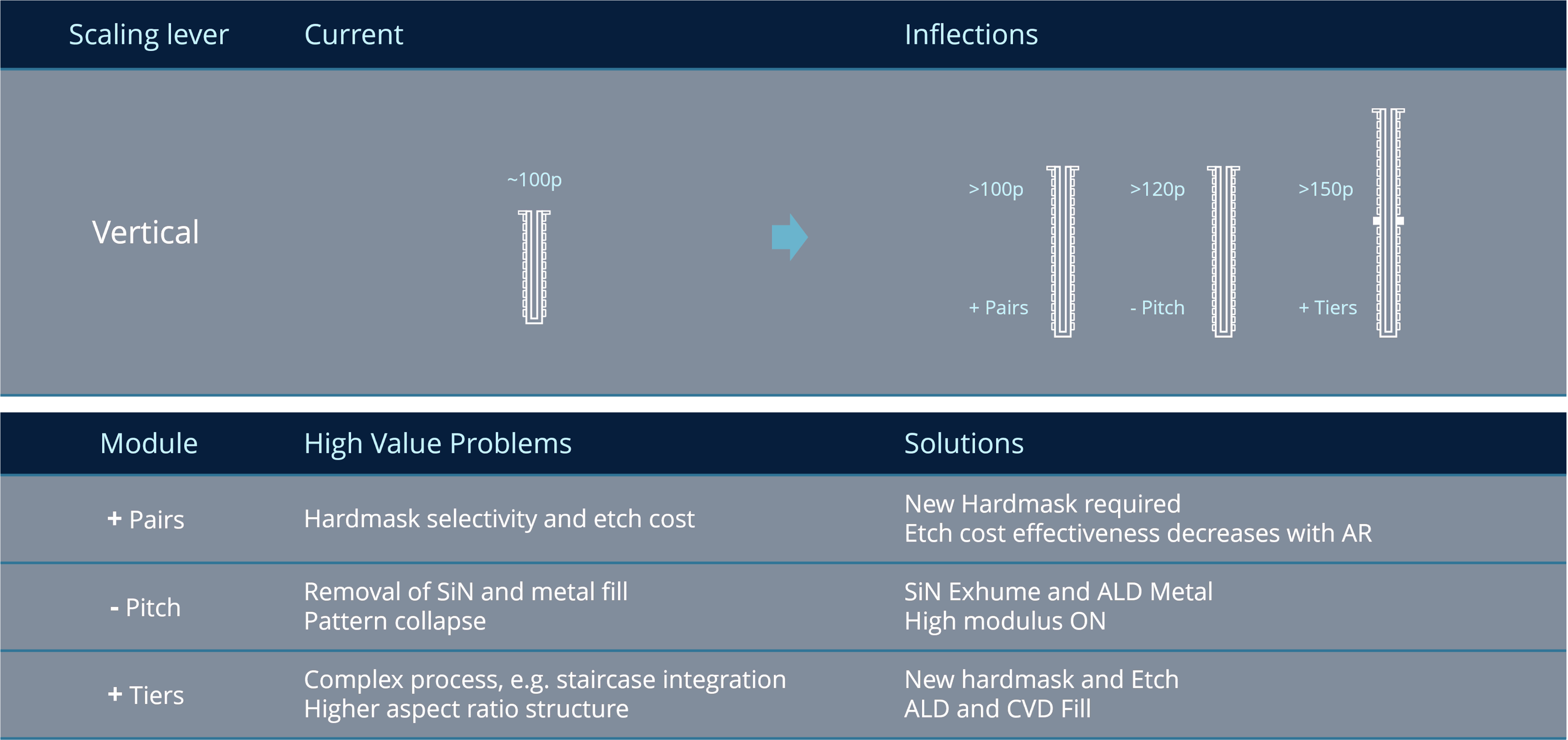
垂直微縮
三維 NAND 微縮的第二種方法是以垂直方向進行。這是透過添加更多對來實現的,但是隨著高度和縱橫比的增加,這變得不那麼成本有效。 縮小每對的厚度可以在相同的堆疊高度上允許更多的層。 但在縮小堆疊高度的過程中,在替換閘極製程中去除硝酸矽並用金屬填充空間變得越來越困難。
隨著對的增加,後處理需要更厚的硬掩模沉積和蝕刻。 更厚的硬遮罩會增加整個堆疊層的高度,導致更高的深寬比。 為了解決這個問題,應用材料公司推出了比傳統硬掩模更具選擇性和低應力的硬掩模薄膜,從而使硬掩模變得更薄。隨著對的增加,後處理需要更厚的硬掩模沉積和蝕刻。 更厚的硬遮罩會增加整個堆疊層的高度,導致更高的深寬比。 為了解決這個問題,應用材料公司推出了比傳統硬掩模更具選擇性和低應力的硬掩模薄膜,從而使硬掩模變得更薄。
在階梯形成後,蝕刻區域必須用介電薄膜加以填充。 這是透過應用材料公司的等離子體增強高深寬比製程或 PE-HARP 介電間隙填充製程來完成的。 這種薄膜具有非常高的沉積速率,具有可調應力,並且與替代方案相比,後處理後的收縮最小。
垂直縮放的下一個關鍵製程是用於高深寬比接觸的金屬間隙填充。在 3D NAND 中,CVD 鎢 (W) 被廣泛用於垂直方向的許多連接。隨著堆疊高度的增加,這種金屬填充工藝面臨兩個挑戰。首先,深觸點具有桶形輪廓。當觸點充滿鎢時,觸點可能會在頂部被夾斷,從而在內部捕獲腐蝕性氣體,這可能會損壞晶片的大部分部件。其次,這些金屬通常在高拉應力下生長,這會使晶圓變形並使鄰近的精細特徵破裂。為了應對這些挑戰,應用材料公司率先推出了接縫抑制鎢技術。該製程包括成核和處理步驟,抑制頂部薄膜的生長,並實現更均勻、無縫的自下而上填充。