解決方案與軟體
半導體 (Semiconductor)
解決方案與軟體
綜合材料解決方案(IMS) 技術
隨著尺寸變小,電阻等界面特性變得比材料的整體特性更重要。 每一個原子層都至為關鍵,而變異性會成為一種阻力。 這需要在真空中整合多種製程,以保護並謹慎設計介面,進而解決效能、功耗和微縮的關鍵瓶頸。
整合材料解決方案或 IMS 技術將多種製程以及客製化計量和感測器結合在一個平台中,幾乎就像晶圓廠中的晶圓廠。應用材料公司正在利用其廣泛的製程技術組合、單元製程領導力和領域專業知識來開發電晶體、互連、記憶體和封裝的整合解決方案。
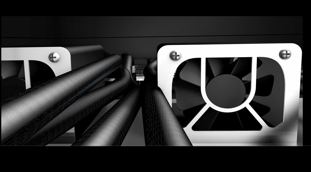
應用材料公司 IMS 技術的最佳範例之一是名為 Endura Copper Barrier Seed IMS系統的材料工程解決方案。它是一種整合材料解決方案,在高真空下將七種不同的製程技術結合在一個系統中: ALD 、 PVD 、 CVD 、銅回流、表面處理、介面工程和計量。該組合取代了保形ALD 透過選擇性ALD ,消除了通孔界面處的高電阻率勢壘。該解決方案還包括銅回流技術,可實現窄特徵中的無空隙間隙填充。通孔接觸界面處的電阻顯著降低,提高了晶片性能和功耗,並使邏輯尺寸能夠持續到3nm及以上。 Endura Copper Barrier Seed IMS 系統現已被全球領先的代工邏輯客戶使用。
Unit Processes, Co-optimization and IMS
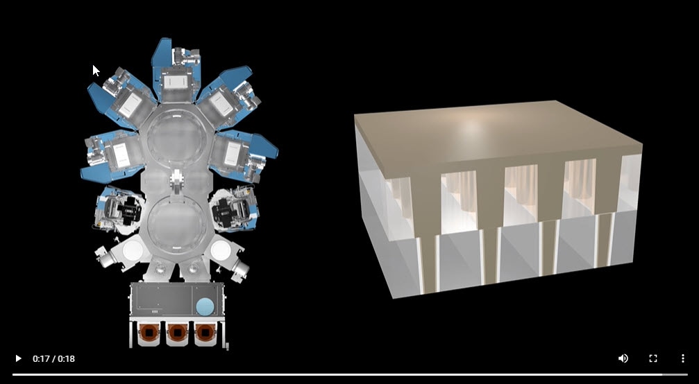
Endura Copper Barrier Seed IMS