市場與轉折點
半導體 (Semiconductor)
解決方案與軟體
異質整合
數十年來,半導體產業始終仰賴二維尺度縮小和積層型半導體整合技術,對晶片效能、功耗以及面積/成本同步進行改善。 但隨著二維尺度縮小技術的放緩並且變得更加昂貴,晶片製造商更趨於轉向異質設計,並在封裝上進行小晶片和元件的整合,以改善功耗、效能、面積、成本和上市時間。
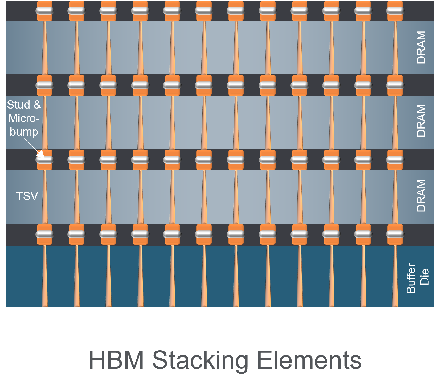
雖然大型主機和 PC 在電子行業中佔據主導地位,但封裝主要用於保護矽晶片並連接到印刷電路板 (PCB)。這裡使用的主要技術是引線鍵結。隨著行動應用程式的發展,封裝不斷發展,以小尺寸提供功能。包裝凹凸 允許兩個平行面之間存在多個連結。必要時,扇出 重新定位連接點,尤其是從晶片上非常緊密的間距到 PCB 上更寬鬆的間距。某些裝置已採用矽通孔 (TSV)允許直接晶片到晶片連接。每項創新都提高了封裝密度,並提供更高的速度和更低的功耗。
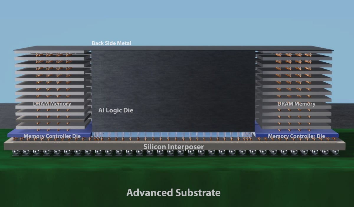
以更低的功耗獲取更多系統級性能的願望促使設計人員考慮如何最好地整合晶片和系統。 設計人員發現很難將高效能運算、機器學習和推理所需的電晶體放置在單一晶片上。 作為替代方法,設計者採用多晶粒封裝技術,使得高效能邏輯與記憶體能更緊密結合,從而降低延遲和功耗。 這種稱為異構整合的方法需要極高的短連接密度,比以前的封裝技術高出幾個數量級。
向異質整合的轉變需要兩個重大突破:
異構設計對於滿足 越來越重要 世界領先的半導體和系統公司的路線圖。 應用材料公司透過我們行業領先的產品組合的獨特廣度和深度以及 行業合作夥伴關係 ,幫助加速這一趨勢 以及 全球最先進的晶圓級封裝實驗室 我們的客戶和合作夥伴與我們一起創新。