Products & Technologies
Products & Services
Contact
Products & Services
Products & Technologies
Services
Resources
Contact
Posted
September 02, 2021

Stay updated on our content.
Heterogeneous Design and Advanced Packaging Enable Advances in PPACt™ Even as Classic Moore’s Law Scaling Slows
.png)
Sep 02, 2021
As a follow-on to my colleague Mike Chudzik’s recent blog, I will preview the second topic to be featured at our Master Class event next week: heterogeneous design and advanced packaging.
For decades, PPAC was enabled by 2D shrinking and monolithic semiconductor integration which delivered simultaneous improvements in chip performance, power and area/cost—just like clockwork. But as classic Moore’s Law 2D scaling slows and becomes more expensive, chipmakers are increasingly moving in the direction of heterogeneous design and on-package integration of chiplets and devices to accelerate PPAC and time to market (PPACt™). Let’s examine the evolving design trends that are enabling this shift and see where the packaging roadmap is headed.
The Rise of Heterogeneous Design
Historically, the primary function of semiconductor packaging was to protect the die and connect it to a printed circuit board (PCB). It was often regarded as a low-value, commodity part of the industry. Also, PCBs served the critical role of routing power and signals between chips and modules. But as computing has progressed from PCs to mobile devices and now the AI era, designers are rethinking how to best integrate both chips and systems. Heterogeneous design and advanced packaging are now a competitive imperative for the world’s leading semiconductor and systems companies.
Fueling this evolution is the paradox that data is growing exponentially while classic Moore’s Law scaling is slowing. We can no longer count on exponential increases in transistor density and speed and like reductions in area/cost. As a result, designers are finding it harder to place all of the transistors they need for high-performance computing, machine learning and inferencing on a single die. As an alternative approach, system designers are seeing the potential to use multi-die advanced packages instead of individually packaged die on a PCB, enabling high-performance logic and memory to be put in closer proximity to reduce latency and power consumption. In short: today, packaging is about more than protection – it’s about PPACt.
Enabling the “PPA” in PPACt …
Compared to the legacy chip on PCB approach, advanced packaging enables substantial increases in I/O density and reductions in latency and power. Using today’s through-silicon vias (TSVs) rather than bump-to-PCB connections, designers can already increase I/O density by approximately 100X and reduce energy per bit transfer by approximately 15X depending on architecture and workload. The next revolution in advanced packaging is hybrid bonding whereby chips and wafers can be directly connected in copper with no need for an interposer. Compared to TSVs, hybrid bonding will enable another 10X increase in I/O density and another 2X improvement in energy per bit.
... and the “Ct” in PPACt
Heterogeneous design can also reduce cost and speed time to market. Monolithic approaches can result in very large die that are expensive to design, debug and tape out. Heterogeneous approaches allow engineers to disaggregate a design into smaller chiplets that can be connected in a single, high-performance package. Smaller die typically have higher yields and lower costs. Also, leading-edge-node wafers are typically more expensive than wafers based on previous nodes, so engineers can mix and match performance-critical die with other chiplets, resulting in a lower blended cost. In addition, proven IP chiplets can be incorporated more quickly. This mix-and-match flexibility can speed time to market.
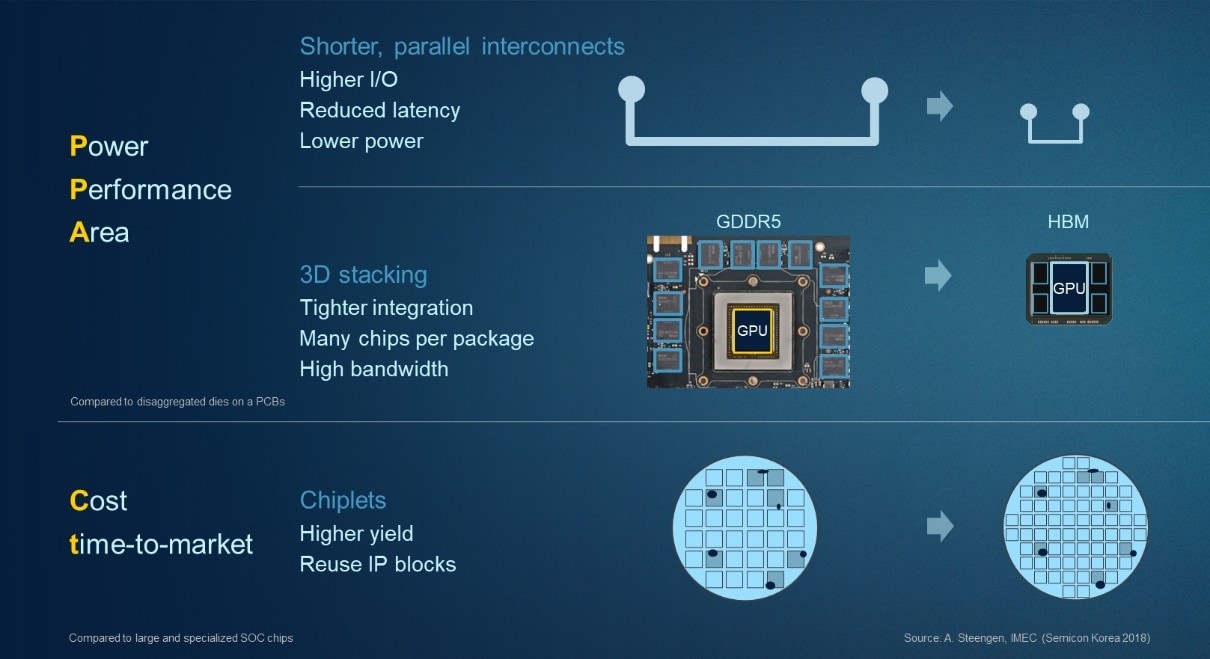
Figure 1: Heterogeneous design and advanced packaging enable PPACt scaling in multiple ways.
Advanced Packaging Increases Demand for Front-End Wafer Fab Equipment
The best way to electrically link multiple chips using the shortest and densest interconnects is with the same front-end wafer fab equipment used to create interconnects within monolithic chips. TSVs increase the use of precision etching, ECD metallization and CMP. Hybrid bonding doesn’t work without special CMP processing, pre-treatments and annealing.
Advanced Packaging Proving Ground
We bring these technologies together at our Advanced Packaging Development Center in Singapore—a state-of-the-art cleanroom that is among the most advanced wafer-level packaging labs in the world. It’s where we enable the foundational building blocks of heterogeneous integration, including advanced bump and micro-bump, fine-line redistribution layer (RDL), TSV and hybrid bonding (see Figure 2). The Center gives us a unique ability to co-optimize process technologies and fully validate their robustness with test vehicles.
.jpg)
Figure 2: Applied Materials enables the foundational building blocks of heterogeneous integration. Each successive technology offers higher input-output density, as well as lower power consumption per bit of data transfer.
Industry Partnerships
Last year Applied announced a joint development agreement with BE Semiconductor Industries N.V. (Besi) to develop the industry’s first complete and proven equipment solution for die-based hybrid bonding. Most of that work is taking place at the Advanced Packaging Development Center, and in next week’s Master Class I will unveil another partnership related to hybrid bonding.
New Larger Substrates Are On the Way
Today’s most advanced packages use silicon wafers as substrates. As designers go for increasingly large and sophisticated packages, 300mm wafers become a limiter. The industry is now eyeing new, rectangular substrates with larger dimensions up to 600mm x 600mm. Applied Materials recently made an acquisition that complements its expertise in PVD to help scale precise metallization across larger substrates. Next week I’ll also share how technology from the display market can help our customers with these larger formats.
In summary, Applied believes heterogeneous design and advanced packaging will be increasingly critical to meeting the PPACt goals of the world’s leading semiconductor and systems companies. We’re helping to accelerate the trend through the unique breadth and depth of our industry-leading portfolio, along with industry partnerships and the world’s most advanced packaging lab where our customers and partners can innovate with us.
Please join us at the Master Class. And for extra credit, find out who made this prediction: “It may prove to be more economical to build large systems out of smaller functions, which are separately packaged and interconnected.”
Tags: PPACt, packaging, Heterogeneous Design, heterogeneous integration, chiplets, Moore's Law
Nirmalya Maity, Ph.D.
Corporate Vice President - Advanced Packaging

Nirmalya Maity is corporate vice president of Advanced Packaging at Applied Materials. Previously, he was at Cabot Corporation where he held several key leadership positions including Chief Technology Officer and vice president of Corporate Strategy & Development. Prior to Cabot, Nirmalya worked for Applied Materials in various technology and product management leadership roles. He received his Ph.D. in chemical engineering from Cornell University and bachelor of science in chemical engineering from the Indian Institute of Technology, Roorkee.

Adding Sustainability to the Definition of Fab Performance
To enable a more sustainable semiconductor industry, new fabs must be designed to maximize output while reducing energy consumption and emissions. In this blog post, I examine Applied Materials’ efforts to drive fab sustainability through the process equipment we develop for chipmakers. It all starts with an evolution in the mindset of how these systems are designed.
Innovations in eBeam Metrology Enable a New Playbook for Patterning Control
The patterning challenges of today’s most advanced logic and memory chips can be solved with a new playbook that takes the industry from optical target-based approximation to actual, on-device measurements; limited statistical sampling to massive, across-wafer sampling; and single-layer patterning control to integrative multi-layer control. Applied’s new PROVision® 3E system is designed to enable this new playbook.
Breakthrough in Metrology Needed for Patterning Advanced Logic and Memory Chips
As the semiconductor industry increasingly moves from simple 2D chip designs to complex 3D designs based on multipatterning and EUV, patterning control has reached an inflection point. The optical overlay tools and techniques the semiconductor industry traditionally used to reduce errors are simply not precise enough for today’s leading-edge logic and memory chips.