半導體 (Semiconductor)
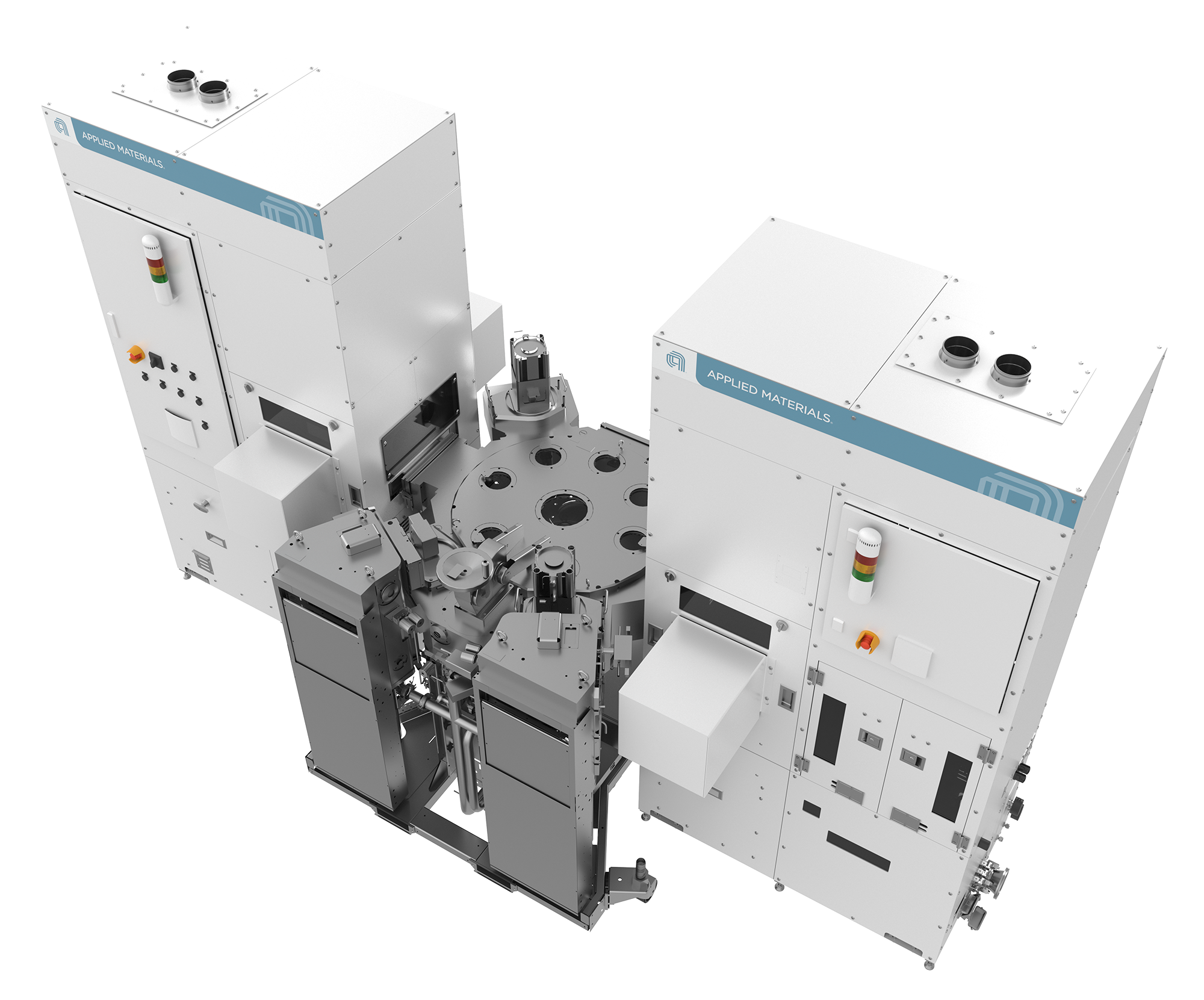
Applied® Picosun® Morpher™ F
Applied® Picosun® Morpher™ F product platform is designed to disrupt the up to 200 mm wafer industries in Beyond and More than Moore technologies. It enables fast, fully automatic, high throughput production of MEMS, sensors, LEDs, lasers, power electronics, optics, and 5G components with the leading process quality, reliability, and operational agility.
Applied® Picosun® Morpher™ F adapts to the changing needs of your industry and the requirements of your customers, on all business verticals from corporate R&D to production and foundry manufacturing. The leading versatility in substrate materials, substrate and batch size, and the wide process range make Morpher truly a transformable, all-inclusive manufacturing facility to keep you spearheading your industry.
Applied® Picosun® Morpher™ F is designed for fully automated handling of wafer batches in combination of industry standard single wafer vacuum cluster platforms. Revolutionary, wafer batch flipping mechanism enables integration of the system with semiconductor manufacturing lines where most of the processing takes place in horizontal geometry, and the SEMI S2/S8 certification ensures that the system is compatible with the strictest standards of the industry.
With our dual-chamber, hot-wall reactor design with fully separated precursor conduits and inlets, we create the highest quality ALD films with excellent yield, low particle levels, and superior electrical and optical performance. The compact, ergonomic design with easy and fast maintenance ensures minimum system downtime and lowest cost-of-ownership in the market.

