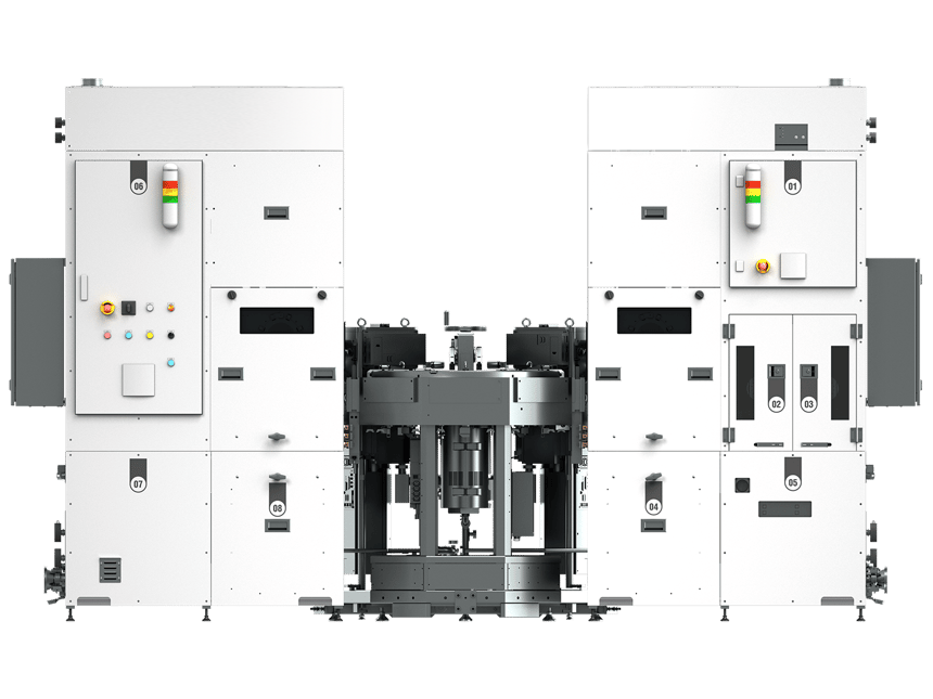
Applied® Picosun® Morpher™ T
Applied® Picosun® Morpher™ T single wafer ALD system is designed to answer the requirements when quality, control and yield come before anything else, for the 200 mm wafer industries. It also enables an enhanced process window for demanding production of MEMS, sensors, LEDs, lasers, power electronics, optics, and 5G components with the leading process quality, reliability, and operational agility.
Applied® Picosun® Morpher™ T offers fully automated handling of wafers and an industry-standard single wafer vacuum cluster platform. It can also be combined with Applied® Picosun® Morpher™ F, batch wafer process module, or with Applied® Picosun® Morpher™ P, plasma enhanced ALD single wafer process module. The state-of-the-art reaction chamber design enables a wide process library even for demanding processes and demanding applications, without deposition on the backside of the substrate for easy process flow integration. Furthermore, the SEMI S2/S8 certification ensures that the system is compatible with the strictest standards of the industry.
The compact, ergonomic design with easy and fast maintenance ensures minimum system downtime and lowest cost-of-ownership in the market. And as a one of its kind, Applied® Picosun® Morpher™ T can be connected to an integrated single VCE and robot to make an extremely low footprint, fully automatic tool for 200 mm substrates.

