半導體 (Semiconductor)
解決方案與軟體
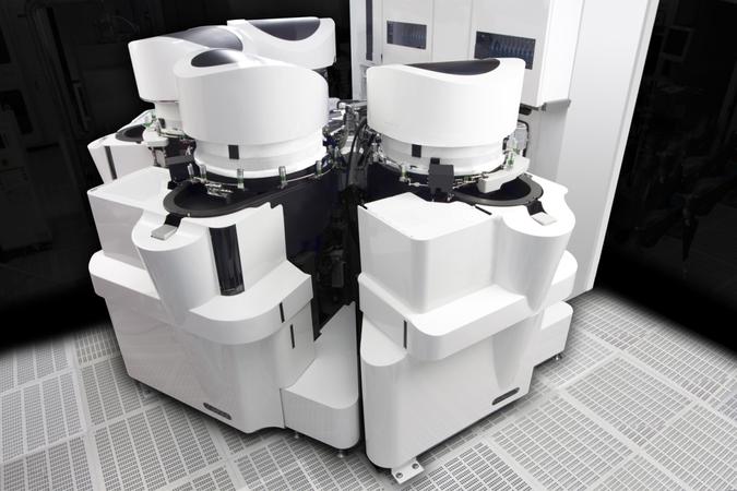
Centura® Tetra™ EUV Advanced Reticle Etch
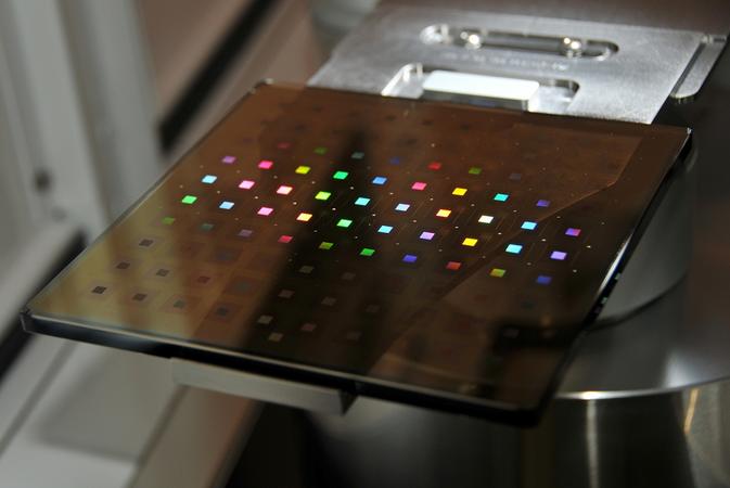
Extreme ultraviolet (EUV) photomasks are used for transferring circuitry patterns onto wafers with new lithography systems using high-energy, short-wavelength light sources. The EUV light source wavelength is approximately 15 times shorter than that of today’s deep ultraviolet lithography, making possible continued feature scaling.
EUV photomasks differ fundamentally from conventional photomasks that selectively transmit 193nm wavelength light to project circuit patterns onto the wafer. At the 13.5nm wavelength used by EUV lithography, all photomask materials are opaque, so the mask contains complex multi-layer mirrors to reflect circuit patterns onto the wafer. These multi-layered EUV masks create unique etch challenges for critical dimensions (CD), profile, line edge roughness, selectivity, and defectivity control while maintaining mask reflectivity.
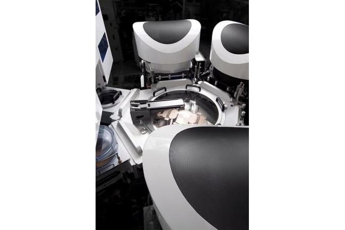
The Centura Tetra EUV system extends Applied’s long-standing mask etch leadership through a design specifically attuned to etch the new materials and complex film stacks used in EUV photomasks, meeting the stringent pattern accuracy, surface finish, and defectivity specifications required to achieve high lithography yields when operating in this reflected mode. The chamber and power-delivery designs complement specialized process chemistries and etch technology, delivering virtually damage-free etch with best-in-class CD uniformity and world-class defectivity control.
The Tetra EUV system is part of Applied Materials’ comprehensive portfolio of lithography-enabling solutions on which the world’s leading mask shops have relied to optimize the productivity and yield of their photomask and lithography operations.


- 1 / 4
- 2 / 4
- 3 / 4
- 4 / 4
