Products & Technologies
Back to Menu
Products & Technologies
Services
Resources
Enlight® Optical Inspection

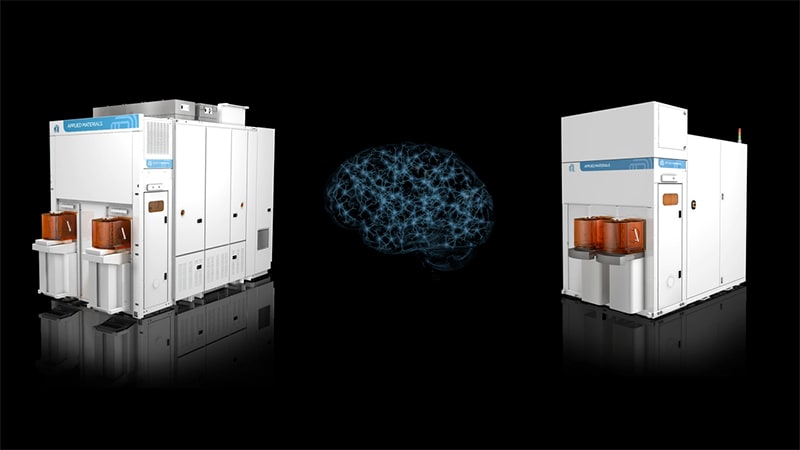
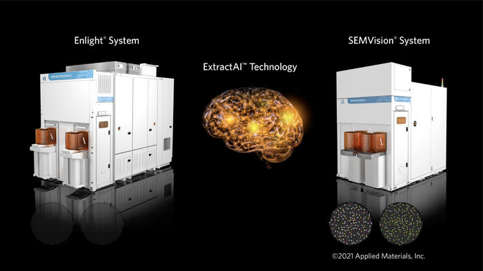
Applied’s Enlight optical inspection, ExtractAI technology, and SEMVision eBeam review together deliver the most actionable data at the fastest rate to accelerate time to market of new process nodes.
As semiconductor design and process complexity has increased, fab costs have soared. Among other things, rising costs have limited the number of inspection steps during the wafer manufacturing sequence. Yet the extremely small feature sizes of leading-edge transistors make yield-killing defects nearly indistinguishable from noise and small variances can accumulate to produce yield-killing defects when fabricating 3D structures and performing complex multi-patterning steps. All these challenges point to the need for more frequent inspection.
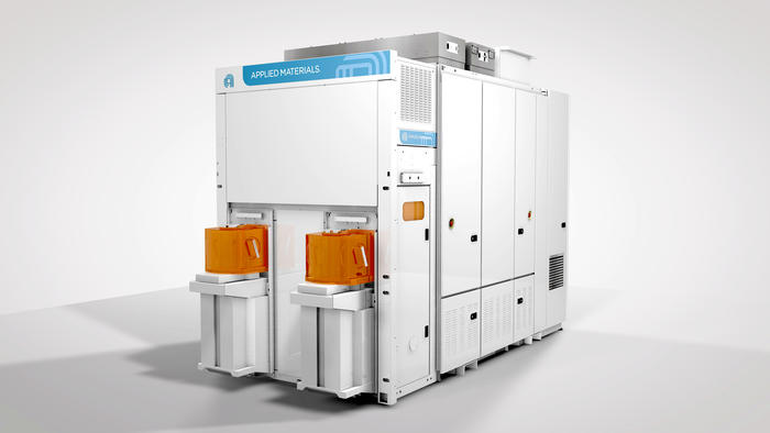
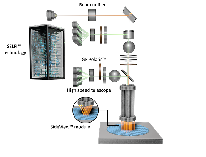
The Enlight Optical Inspection system is part of Applied’s approach to reinventing process control so that chipmakers can achieve the required extreme inspection sensitivity, inspect more often, collect more data, accelerate yields, and lower the cost per wafer. The system combines industry-leading speed with high resolution and advanced optics that capture more data per scan. Its unique architecture features the highest numerical aperture on the market to achieve a high-resolution scan and unique 3D polarization control that suppresses wafer noise. It is also the only system with simultaneous brightfield and greyfield detection channels and flexible image computing. All these features enable generation of high-quality Big Data in production.
By generating Big Data, the Enlight system achieves a 3X reduction in the cost of capturing critical defects. This lower cost of ownership allows chipmakers to increase the number of inspection steps in fabrication and conduct quick, accurate root cause determination. Big Data also allows chipmakers to conduct line monitoring for timely excursion prediction and detection.
Integral to Applied’s approach, Applied’s breakthrough ExtractAI™ technology works with the Enlight system’s Big Data to solve the most difficult challenge of inspection: distinguishing the yield-killing defects from the noise. Using machine learning and statistical processing algorithms, ExtractAI uniquely creates a real-time connection between the Enlight system and Applied’s market-leading eBeam review and classification SEMVision® system. This technology is exceptionally efficient. It can extract all defects of interest on a wafer after guiding SEMVision, defect by defect, through only 0.001X of potential defects. ExtractAI learns in real time and increasingly rapidly creates fully classified and completely noise-free wafer defect maps as successive wafers are processed.
Combining Applied’s Enlight optical inspection, ExtractAI technology, and SEMVision eBeam review capabilities, fabs receive more actionable data, faster than ever before, lowering their cost of ownership and accelerating yields and time to market.


- 1 / 3
- 2 / 3
- 3 / 3
