Products & Technologies
Products & Services
Company
Contact
Products & Services
Products & Technologies
Services
Resources
Company
Contact
Semiconductor
Patterning
Technologies
Software
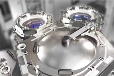
Epitaxy
Epitaxy is used in semiconductor fabrication to create a perfect crystalline foundation layer on which to build a semiconductor device, to deposit a crystalline film with engineered electrical properties, or to alter mechanical attributes of an underlayer in a way that improves its electrical conductivity.
This last application is known as strain engineering in which the epitaxial film results in compressive or tensile strain in the lattice of the transistor channel. Applied’s epi technologies address all of these applications, producing highly uniform films with precise placement of dopant atoms, exceptionally low defect levels, and the capability for selective deposition.