半导体 (Semiconductor)
解决方案与软件
混合键合
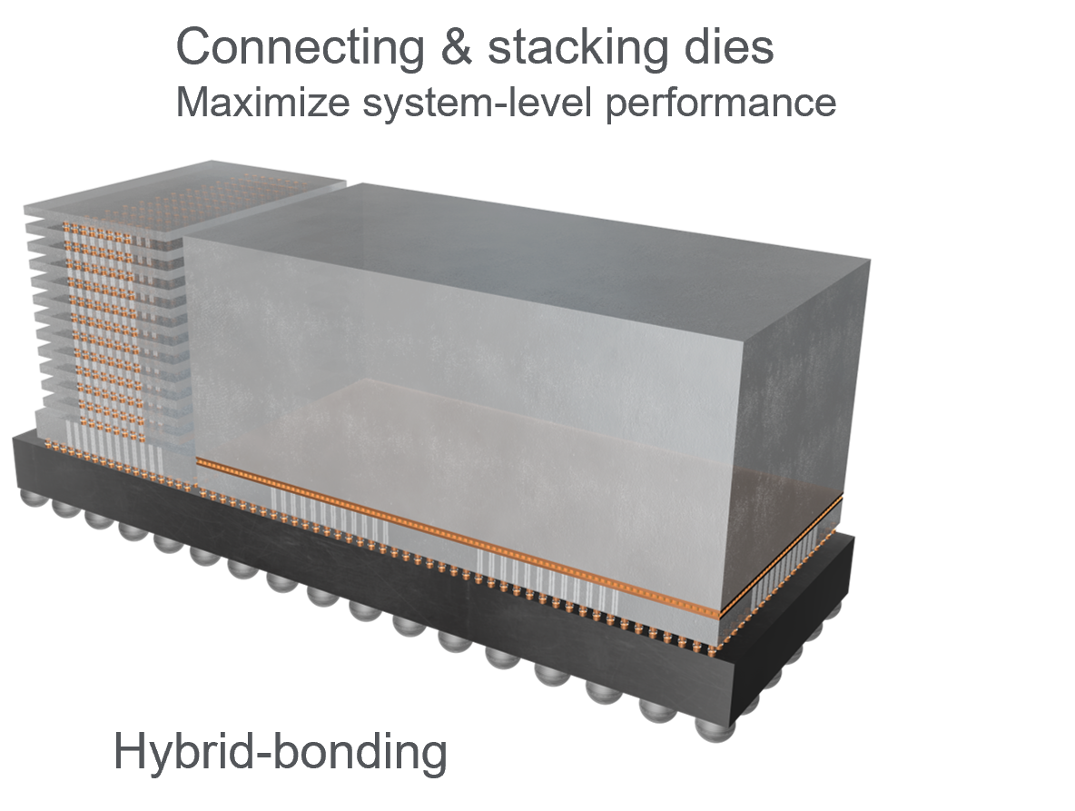
异构集成技术帮助半导体公司将不同功能、技术节点和尺寸的芯粒集成到先进封装中,使这些组合起来的多个芯粒像单一芯片那样工作。高性能计算和人工智能等应用对晶体管的需求持续以指数级速度增长,而传统的二维微缩技术缩小晶体管的能力正在放缓,成本也越来越高——异构集成解决了这一行业难题。 它是新战略的核心组成部分,可帮助芯片制造商以全新方式改善芯片性能、功耗、面积、成本和上市时间(PPACt)。
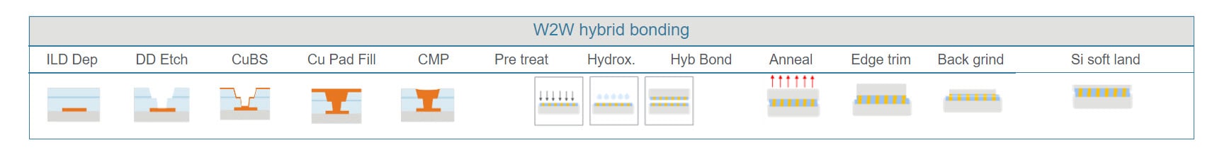
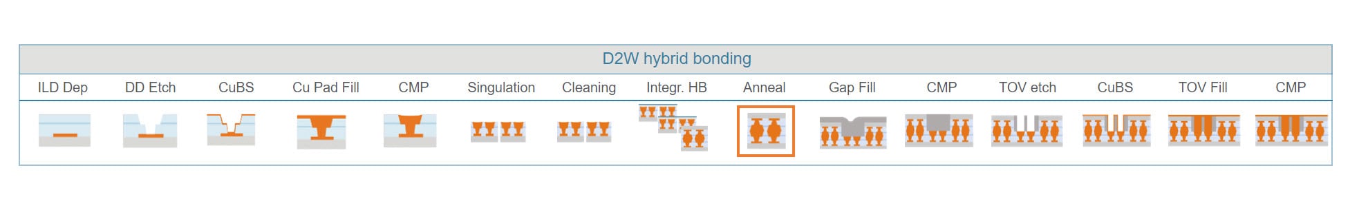
芯片制造商可以利用硅通孔(TSV)和/或混合键合将芯粒集成到先进的 2.5D 和 3D 封装中。与传统的 PCB 方案的芯片相比,硅通孔使设计人员能够显著提高性能并降低功耗。最新的封装创新技术——混合键合,可实现芯片或晶圆之间的直接连接。与 TSV 相比,混合键合可进一步提高性能并降低功耗。在混合键合中,晶粒逐一堆叠,这些晶粒之间使用极细间距的铜-铜互连提供连接。
铜-铜混合键合可实现与单片设计非常接近的性能,而且功耗和信号传输也几乎不受影响。技术挑战在于以更低的成本实现无缺陷的铜-铜键合,而且芯片-芯片对齐误差几乎为零。这需要对上游和下游工艺制程以及器件设计实施重大改动。I在这方面,工艺整合的发展和协同优化起着至关重要的作用。
应用材料公司拥有多种技术和解决方案,包括 电介质 沉积 、 金属沉积 、 电镀 、 化学机械平坦化 (CMP) 和 刻蚀 ,以支持混合键合工艺流程的各个阶段。应用材料公司的 Insepra™ SiCN 和 Catalyst CMP 系统可利用新材料和增强型表面制备实现先进的混合键合。
我们还与开发伙伴合作,为客户提供技术,以开发和推广完整的端到端混合键合解决方案。
第一项合作是晶圆到晶圆,用于 CIS 和 NAND,也可能用于 DRAM。应用材料公司正在 与 EVG 合作开发晶圆到晶圆混合键合的集成工艺。