Products & Technologies
Products & Services
Contact
Products & Services
Products & Technologies
Services
Resources
Contact
Posted
January 10, 2022

Stay updated on our content.
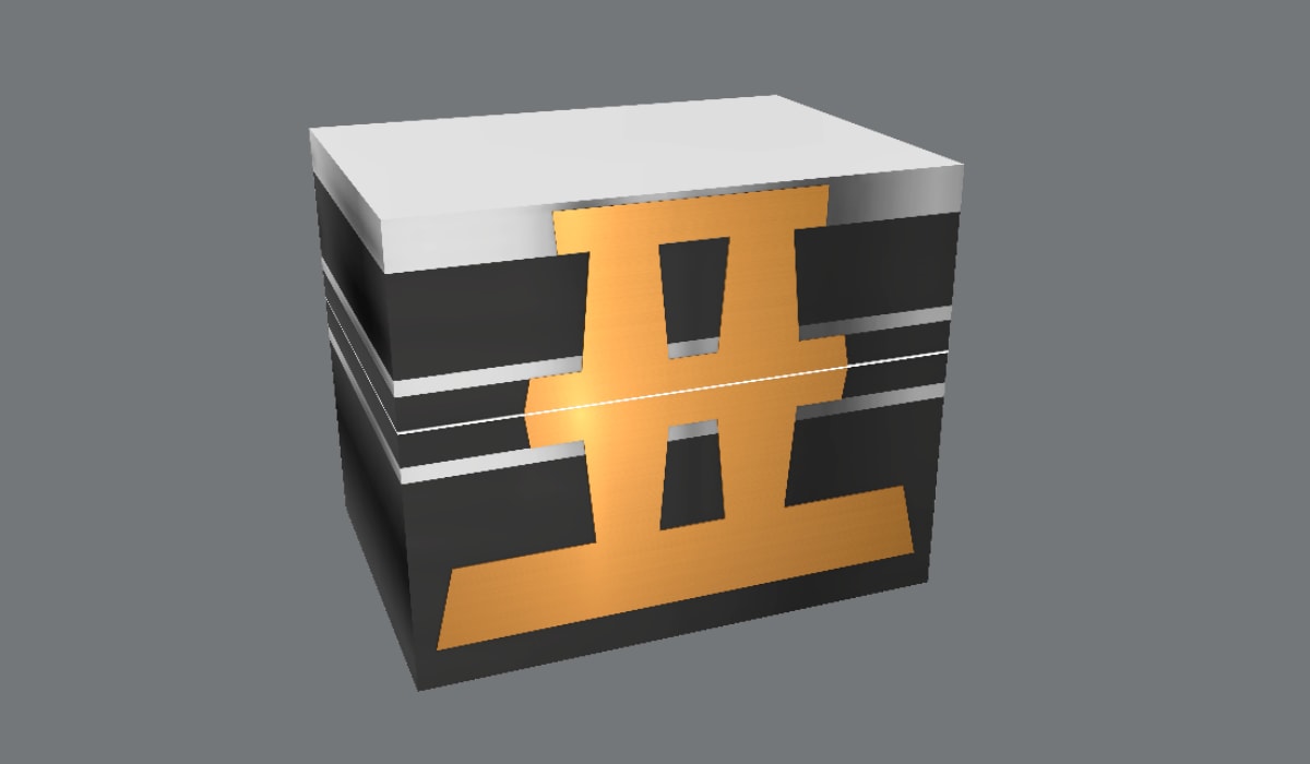
Expanding the Ecosystem for Hybrid Bonding Technology
Jan 10, 2022
A key part of our strategy at Applied Materials is to be the PPACt enablement company™ for our customers. We offer the broadest portfolio of products that deliver improvements in chip power, performance, area, cost and time-to-market. As traditional Moore’s Law scaling slows and becomes more expensive, new design and manufacturing paradigms are being adopted by chipmakers and systems companies to advance their PPACt roadmaps. A prime example is the increasing use of heterogeneous design and advanced packaging solutions.
As I’ve stated in a previous blog, semiconductor packaging used to be about protecting the die and connecting it to a printed circuit board (PCB). Today, advanced packaging enables heterogeneous design and integration which allows chips manufactured on various nodes and for different functions to be combined in a single package. Heterogeneous design delivers simultaneous improvements in PPACt and provides greater design and manufacturing flexibility.
Applied Materials’ Advanced Packaging Development Center in Singapore.
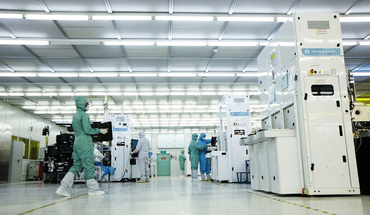
Advanced packaging has been a focus area of Applied Materials for many years. We are the largest supplier of advanced packaging technologies with optimized products spanning etch, PVD, CVD, electroplating, surface treatments and annealing. Much of our work in this area takes place at our Advanced Packaging Development Center in Singapore—a state-of-the-art cleanroom that is among the most advanced wafer-level packaging labs in the world. It’s where we work closely with customers and ecosystem partners to accelerate development of the foundational building blocks of heterogeneous integration.
One of our key R&D collaborators at the Center is the Institute of Microelectronics (IME), a research institute of Singapore’s Agency for Science, Technology and Research (A*STAR). We recently entered into a new phase of our collaboration with A*STAR’s IME, which includes a combined investment of approximately $210 million to upgrade and expand the Advanced Packaging Development Center to accelerate materials, equipment and process technology solutions for hybrid bonding and other emerging, 3D chip integration technologies. The expansion provides semiconductor and systems companies with a complete suite of tools and technologies for developing and prototyping hybrid bonding packaging designs.
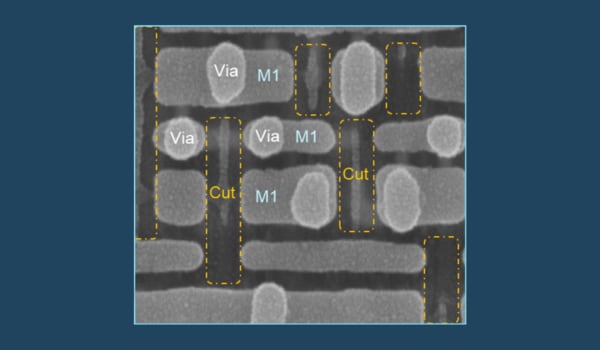
Hybrid bonding is a major improvement from conventional multi-chip packaging techniques whereby I/O pins are connected to a substrate using metal bumps, with the substrate’s wiring used to complete the electrical interconnections between chips. Hybrid bonding connects chips and wafers with direct copper-to-copper bonding, thereby reducing wiring distances and increasing I/O density. This improves power efficiency and enables greater system performance (see Figure 1).
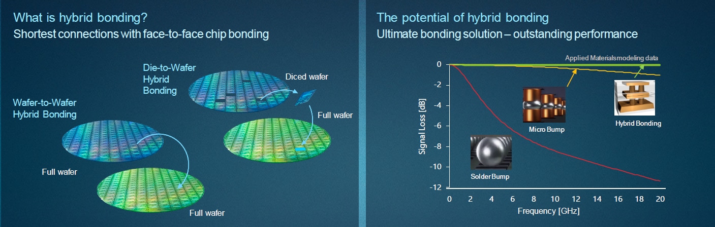
Figure 1: Hybrid bonding eliminates the need for bumps and micro-bumps, enabling performance that is very close to monolithic designs with almost no power and signal penalties.
To enable hybrid bonding requires a broad suite of semiconductor manufacturing technologies. To achieve the best performance, key technologies for bond-pad formation, planarization, surface preparation and bonding should be co-optimized. Our latest work with A*STAR’s IME complements the die-to-wafer and wafer-to-wafer hybrid bonding collaborations Applied currently has underway with other industry partners. Our intent with these engagements is to build an ecosystem that can accelerate our customers’ PPACt roadmaps and strengthen Applied’s leadership in advanced packaging solutions.
Tags: PPACt, packaging, Heterogeneous Design, heterogeneous integration, hybrid bonding, Advanced Packaging Development Center, A*STAR, IME
Nirmalya Maity, Ph.D.
Corporate Vice President - Advanced Packaging

Nirmalya Maity is corporate vice president of Advanced Packaging at Applied Materials. Previously, he was at Cabot Corporation where he held several key leadership positions including Chief Technology Officer and vice president of Corporate Strategy & Development. Prior to Cabot, Nirmalya worked for Applied Materials in various technology and product management leadership roles. He received his Ph.D. in chemical engineering from Cornell University and bachelor of science in chemical engineering from the Indian Institute of Technology, Roorkee.

Adding Sustainability to the Definition of Fab Performance
To enable a more sustainable semiconductor industry, new fabs must be designed to maximize output while reducing energy consumption and emissions. In this blog post, I examine Applied Materials’ efforts to drive fab sustainability through the process equipment we develop for chipmakers. It all starts with an evolution in the mindset of how these systems are designed.
Innovations in eBeam Metrology Enable a New Playbook for Patterning Control
The patterning challenges of today’s most advanced logic and memory chips can be solved with a new playbook that takes the industry from optical target-based approximation to actual, on-device measurements; limited statistical sampling to massive, across-wafer sampling; and single-layer patterning control to integrative multi-layer control. Applied’s new PROVision® 3E system is designed to enable this new playbook.
Breakthrough in Metrology Needed for Patterning Advanced Logic and Memory Chips
As the semiconductor industry increasingly moves from simple 2D chip designs to complex 3D designs based on multipatterning and EUV, patterning control has reached an inflection point. The optical overlay tools and techniques the semiconductor industry traditionally used to reduce errors are simply not precise enough for today’s leading-edge logic and memory chips.