Products & Technologies
Products & Services
Contact
Products & Services
Products & Technologies
Services
Resources
Contact
Enabling Innovation Beyond Shrinking Transistors
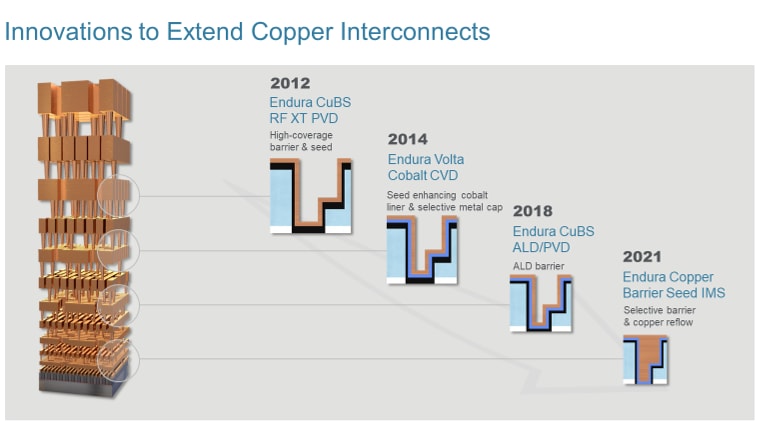
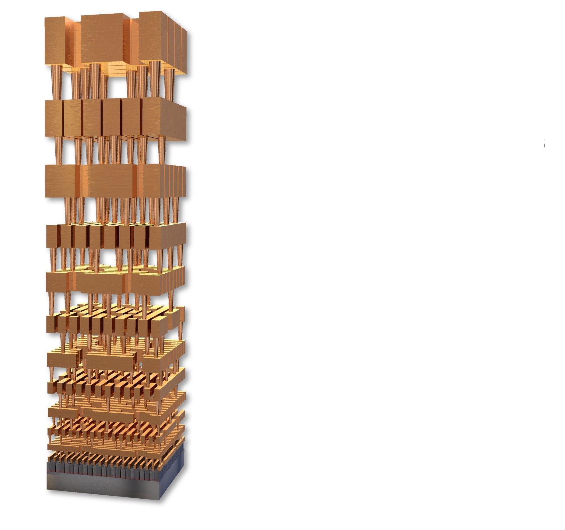
Logic scaling requires more than shrinking transistor size alone—innovations in the transistor contact and chip interconnect modules are necessary as well. A smartphone processor has over 16 billion transistors and over 32 billion via and contact connections. It also has over 10 layers of metals of varying dimensions, with the ones closest to the transistors being the narrowest.
Transistors, which act as switches, are connected electrically through metal contacts that are then interconnected by copper wires, or copper interconnects. These interconnects distribute power and route logic signals. As transistor dimensions shrink, interconnect resistance increases dramatically, impacting device power and performance, necessitating continuous advances in materials and process technologies.
As the leader in interconnect process technology, Applied Materials enables innovations in this area with our successful suite of products in metals deposition. The Endura® Copper Barrier IMS® system with selective barrier deposition and reflow copper technologies is crucial in enabling contacts and interconnects necessary to enable logic scaling to continue at 3nm and beyond.
To continue scaling beyond the 2nm node, major breakthroughs in interconnect and contact design, as well as process technologies, are necessary. Backside power delivery is one such innovation.
More information on Interconnects can be found on our Master Class and blogs on this topic.