Products & Technologies
Products & Services
Contact
Products & Services
Products & Technologies
Services
Resources
Contact
Posted
June 14, 2021

Stay updated on our content.
Challenges to Interconnect Scaling at 3nm and Beyond
Jun 14, 2021
The previous blog in this series, authored by my colleague Mike Chudzik, previewed Applied’s upcoming Logic Master Class with a focus on transistor design and the physical limitations that must be overcome to enable advanced logic scaling. I will continue the discussion by outlining some of the key challenges of scaling the interconnects that bring signals and power to the discrete devices that make up the IC.
Interconnects consist of two key metal components: the metal lines that transfer current within the same device layer and the metal vias that transfer current between layers. Pitch reduction narrows the width of both and increases resistance along with the time needed to move signals across distances. It also increases the voltage drop across a circuit, throttling circuit speed and increasing power dissipation.
While transistor performance improves with scaling, the same cannot be said for interconnect metals. In fact, as dimensions shrink, interconnect via resistance can increase by a factor of 10 (see Figure 1). This results in resistive-capacitive (RC) delays that reduce performance. It also increases power consumption.
Interconnects consume close to one third of device power and account for more than 75 percent of RC delay, so improving interconnect resistance is the best way to improve overall device performance.
Left unchecked, resistance issues can fully negate the benefits of transistor improvements.
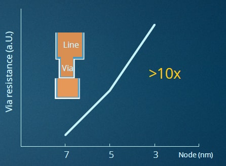
Figure 1: Interconnect via resistance increases as process nodes get smaller, which compromises device performance and power consumption.
The key to improving interconnect resistance at small geometries is developing new metal fill processes that minimize or entirely eliminate high resistivity barriers and liners. Thinning or eliminating these barriers and liners reduces interface resistance and maximizes the volume available for metal conductors.
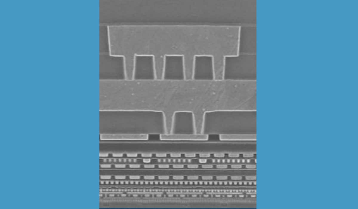
A typical copper interconnect structure is built using three films (see Figure 2). A tantalum-nitride (TaN) barrier is deposited on the sidewalls, which are made of a dielectric material, providing for good adhesion and preventing the copper from diffusing into the dielectric. Then a Cobalt (Co) liner is deposited: it adheres to the TaN barrier and facilitates subsequent copper (Cu) fill. Cu is deposited into the remaining volume using a process called copper reflow.
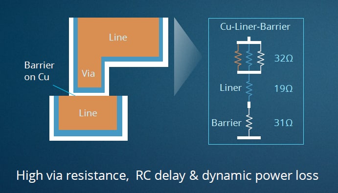
Figure 2: The three films of a typical copper interconnect structure: TaN barrier (white), Co liner (blue) and Cu fill (orange).
So, what is needed to further scale the interconnect?
The TaN/Cu interface is the largest contributor to the via’s overall resistance. The best way to reduce the resistance would be to eliminate this interface altogether, but this could only be accomplished by developing a selective barrier deposition process.
Another increasing challenge of the liner-barrier approach is that as the via volume shrinks with scaling, the liner-barrier takes up a larger percentage of the available space and reduces the space available for conductive Cu. The ideal solution would be an entirely new Cu reflow technology. At our upcoming Logic Master Class, I’ll discuss these issues further and provide details about unique innovations from Applied Materials.
An Entirely New Architecture Promises Further Breakthroughs
Scaling interconnects beyond the 2nm node will require additional design breakthroughs. One area of focus involves the way power is delivered to the transistors.
Each logic chip is made up of standard cells, which are groups of transistors and interconnect structures that provide specific logical functions. Each cell needs space for signal lines along with a power rail that delivers current from an external power supply to the transistor. The power rail is typically 3 times larger than the smallest interconnect wire, which makes it a major contributor to cell size (see Figure 3).
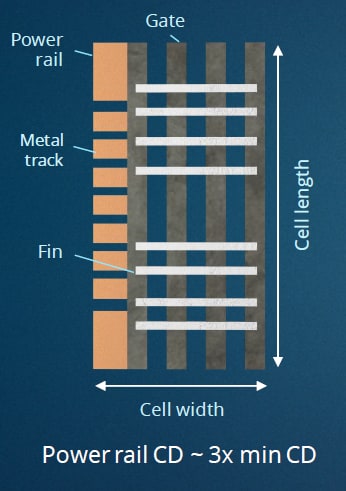
Figure 3: The power rail is typically three times larger than the smallest interconnect wire, making it is a major contributor to cell size.
In addition, to reach the transistors, the power delivery network is routed through all of the metal levels of the chip, and there can easily be 12 or more. At each level, metal resistance causes a significant drop in the supply voltage. Designers can cope with cumulative voltage losses of around 10 percent. But because resistance is increasing with each node shrink, it is projected that without a new architecture, the power distribution network could consume 50 percent of the incoming supply voltage.
To enable logic scaling to continue, the industry is developing a new architecture called buried power rail with backside power delivery network (see Figure 4). This architecture routes power to the transistor cell from the back side of the silicon wafer, beneath the transistors. The approach is expected to provide three important benefits: improving voltage losses by as much as 7X; allowing the transistor cell area to be scaled by 20-33 percent; and leaving more cell space for the signal lines which also incur resistance from scaling.
Additional details on how Applied Materials is helping enable the buried power rail inflection will also be shared at the Logic Master Class.
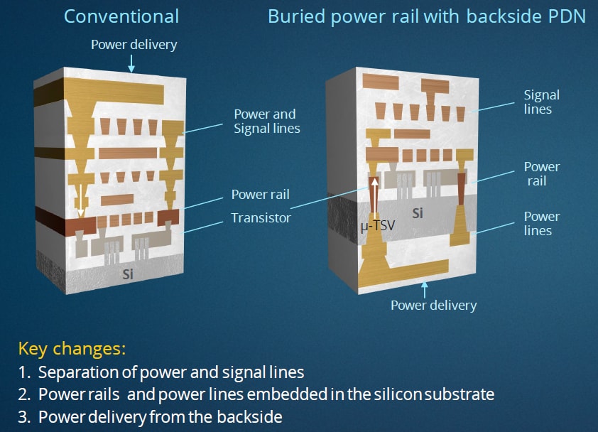
Figure 4: The new buried power rail with backside power delivery network architecture moves the power distribution network to the back side of the silicon wafer, beneath the transistors. It enables further scaling of transistor cell areas and allows signal lines to remain larger and have lower resistance.
Final Thoughts
Improving PPACt in logic devices requires concurrent innovations in transistors, contacts and interconnects. The conventional approaches are being pushed to the limit, but we already envision solutions that will be enabled by new materials and materials engineering techniques. Many of these are in Applied’s sweet spot as we have the broadest portfolio of technologies spanning materials creation, modification, removal and analysis. We can also combine these technologies in unique and highly enabling ways that no one else can.
Tags: interconnect, scaling, RC delay, buried power rail, logic, PPACt, copper reflow
Mehul Naik, Ph.D.
Master and Vice President of Technology, Semiconductor Products Group

Mehul Naik is a Master and Vice President of Technology with the Advanced Product Technology Development team in the Semiconductor Products Group at Applied Materials. He is responsible for the Logic Program working on inflection mapping and leading cross-functional programs in the FEOL, MEOL and Interconnect area. He has authored over 64 publications and holds over 90 U.S patents. Mehul earned his Ph.D. in chemical engineering from Rensselaer Polytechnic University.

Adding Sustainability to the Definition of Fab Performance
To enable a more sustainable semiconductor industry, new fabs must be designed to maximize output while reducing energy consumption and emissions. In this blog post, I examine Applied Materials’ efforts to drive fab sustainability through the process equipment we develop for chipmakers. It all starts with an evolution in the mindset of how these systems are designed.
Innovations in eBeam Metrology Enable a New Playbook for Patterning Control
The patterning challenges of today’s most advanced logic and memory chips can be solved with a new playbook that takes the industry from optical target-based approximation to actual, on-device measurements; limited statistical sampling to massive, across-wafer sampling; and single-layer patterning control to integrative multi-layer control. Applied’s new PROVision® 3E system is designed to enable this new playbook.
Breakthrough in Metrology Needed for Patterning Advanced Logic and Memory Chips
As the semiconductor industry increasingly moves from simple 2D chip designs to complex 3D designs based on multipatterning and EUV, patterning control has reached an inflection point. The optical overlay tools and techniques the semiconductor industry traditionally used to reduce errors are simply not precise enough for today’s leading-edge logic and memory chips.