Products & Technologies
Products & Services
Contact
Products & Services
Products & Technologies
Services
Resources
Contact
Enabling the Continued Miniaturization of Transistors
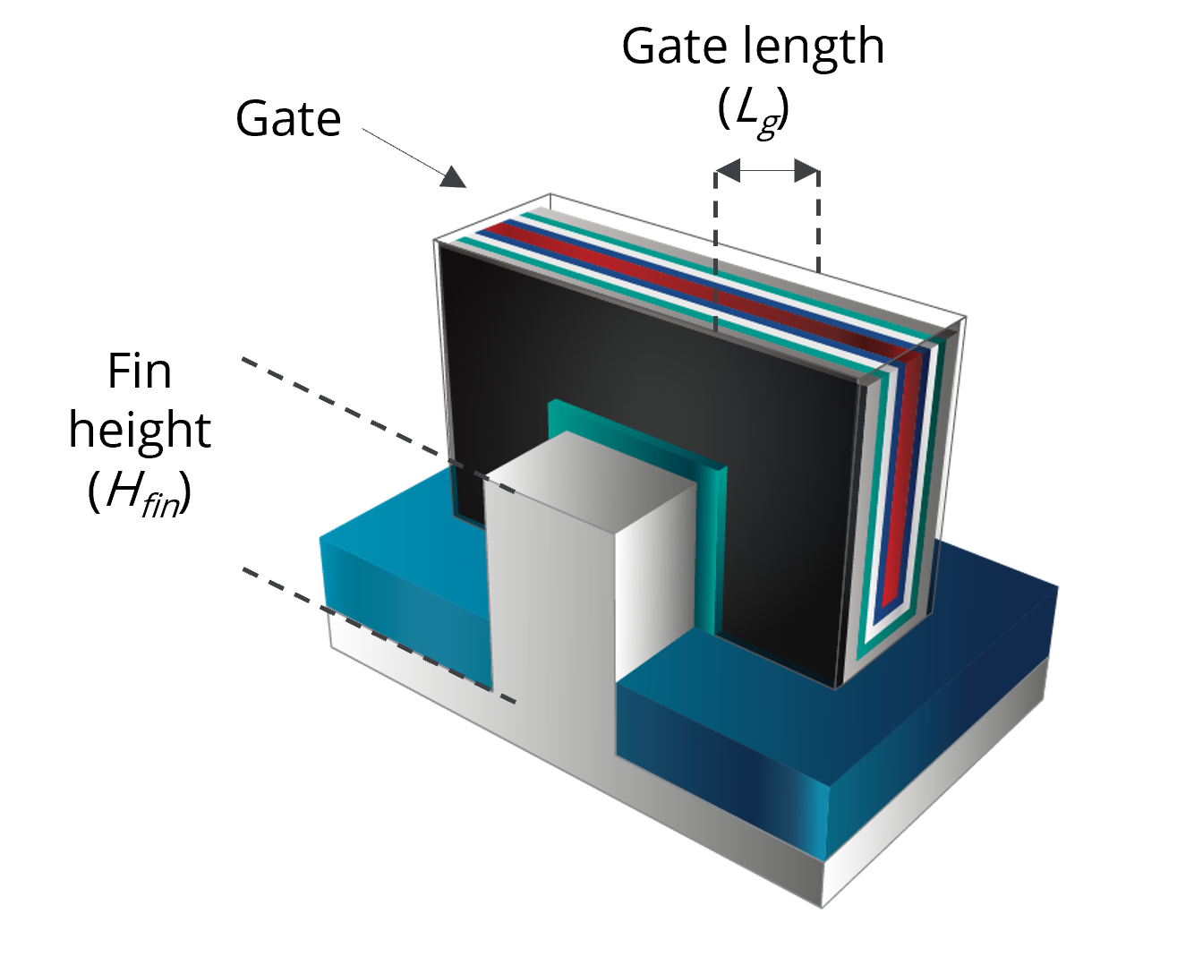
FinFET, short for Fin Field-Effect Transistor, is an advanced transistor architecture used in semiconductor devices, particularly in integrated circuits (ICs) such as microprocessors, graphics processing units (GPUs), and system-on-chips (SoCs).
In a FET, the drain-to-source current flows via a conducting channel that connects the source region to the drain region. The vertical fin-like structure of the channel gives this design the name FinFET. The gate electrode in a FinFET surrounds the channel on three sides, providing better control over the flow of current through the channel, compared to a planar design. This results in reduced leakage current, thereby improving performance and power efficiency.
FinFETs scale efficiently and allow for the continued miniaturization of transistors. With our broad portfolio of products spanning deposition, etch, patterning, and metrology and inspection, Applied Materials plays a key role in enabling the development and manufacturing of FinFET technology.
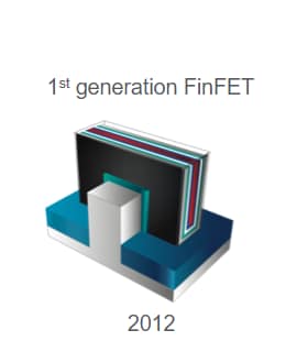
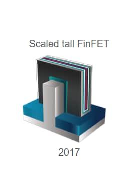
As FinFETs have scaled for smaller geometries, the fins have become narrower and taller, and the FinFET architecture is being pushed to its limits. The industry is looking to a new architecture called gate-all-around or GAA to push performance and power efficiencies even further.
More information on FinFETs can be found on our MasterClass and blogs on this topic.