Products & Technologies
Products & Services
Contact
Products & Services
Products & Technologies
Services
Resources
Contact
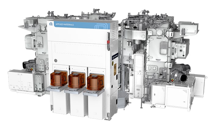
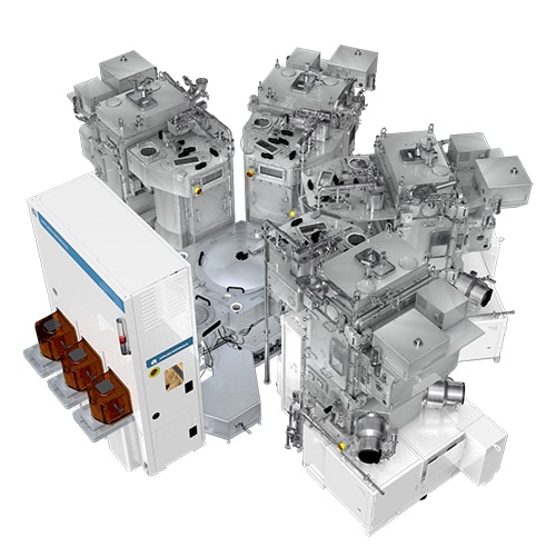
Centura Sculpta Pattern-Shaping System
The Applied Centura™ Sculpta™ patterning system makes possible a novel capability called pattern shaping, defined as precisely and unidirectionally modifying the dimensions of on-wafer features to enhance the performance of EUV patterning. Sculpta is intended for the most critical patterning layers in advanced logic nodes. It can be used to reduce the complexity of patterning schemes to realize Power, Performance, Area, Cost, and time to market (PPACt™) benefits – a valuable addition to the patterning engineer’s toolbox.
- 1 / 2
- 2 / 2