Products & Technologies
Products & Services
Contact
Products & Services
Products & Technologies
Services
Resources
Contact
Posted
February 17, 2023

Stay updated on our content.
Bringing the Future of Advanced Patterning into Focus at SPIE
Feb 17, 2023
This year’s SPIE Advanced Lithography + Patterning conference in San Jose, Calif. (Feb. 26 – March 2) comes at a time when the semiconductor industry needs new breakthroughs to solve the patterning challenges of continued scaling with EUV lithography which will become more intense with the arrival of High-NA EUV. In this blog, I will discuss two of these challenges and give a preview of the exciting events Applied Materials has planned during the conference.
Patterning Challenge 1: Reducing the Cost, Complexity and Environmental Impact of Advanced Patterning
As my colleague, Regina Freed, noted in a previous blog, chip designers are pushing the limits of advanced lithography by creating patterns that are tighter than the resolution limits of EUV in order to squeeze more transistors, contacts and interconnect wires onto a chip. After all, more transistors enable higher performance and tighter device spacing optimizes die area and cost.
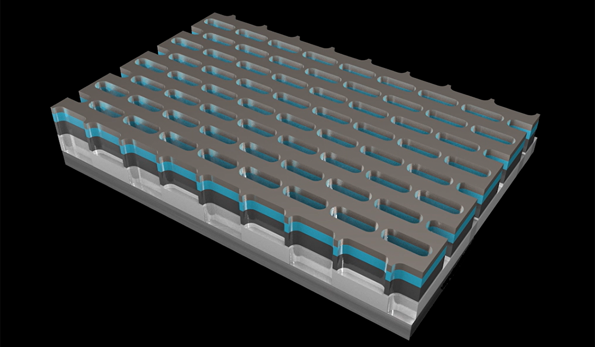
Using EUV double-patterning, chipmakers split a high-density design onto two mask patterns that each adhere to the spacing limits of EUV. Both patterns are transferred to intermediate films and then etched into the wafer. While EUV double-patterning is effective at increasing feature density, it adds design and patterning complexity along with process steps that consume time, energy, materials and water – and increase the cost of wafer fabs and wafer production. It also introduces the risk of alignment errors between the two mask patterns, which can degrade chip performance and power efficiency, and reduce yield.
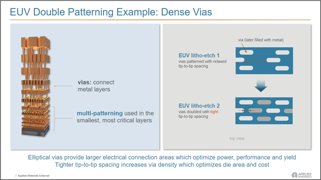
Imagine the benefits to the industry if we could somehow use materials engineering to reshape EUV patterns, reducing spacing and increasing density without the need for a second EUV step? There could be substantial savings in cost, complexity, cycle times, and energy and materials consumption. At SPIE, we’ll discuss how.
Patterning Challenge 2: Controlling EUV and High-NA EUV Lithography and Etch Processes
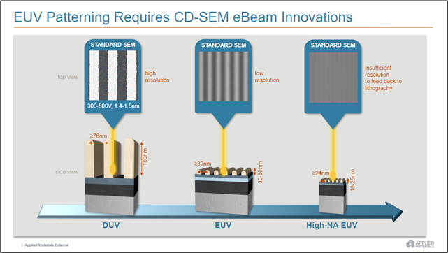
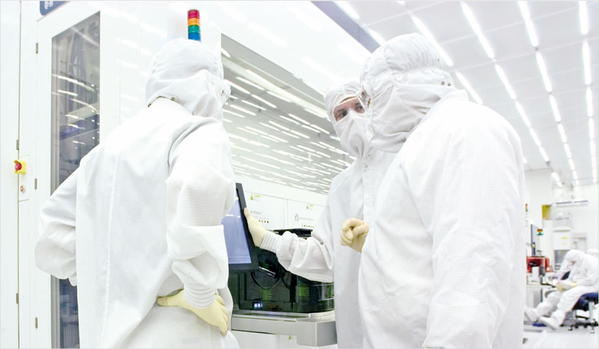
When it comes to measuring semiconductor device features, the CD-SEM (critical dimension scanning electron microscope) is often called “the ruler of the fab” because it produces the most precise, sub-nanometer measurements available. CD-SEMs are used to measure the critical dimensions of patterns, such as lines and spaces, once the scanner transfers them from mask to photoresist. These measurements continuously calibrate the lithography scanner and process to ensure the patterns are correct before they are etched into the wafer.
Likewise, CD-SEMs are used after etch to correlate intended patterns with on-wafer results. CD-SEMs thereby help control the etch process – and enable a feedback loop between lithography and etch that gives engineers highly correlated data sets for holistic process tuning.
Measuring the critical dimensions of device features becomes more challenging as photoresists get thinner with EUV and especially High-NA EUV. We need thinner photoresists to enable mask patterns to be developed with the 10X fewer photons available as compared to deep UV. Also, thinner resists help prevent the densely packed lines formed with EUV from collapsing onto one another.
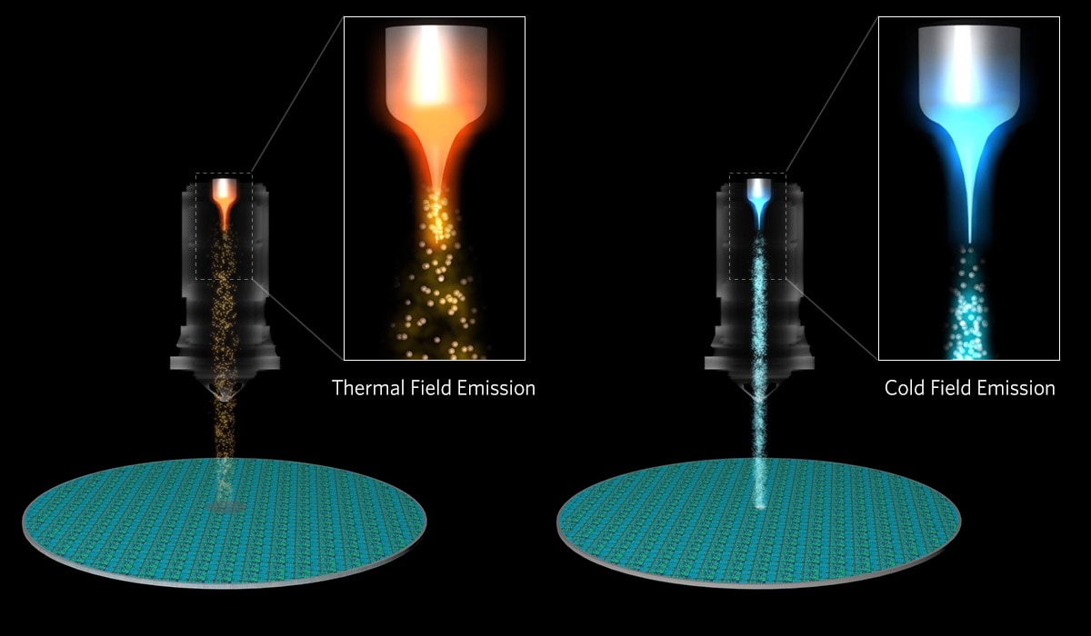
But to capture accurate measurements, the CD-SEM must be able to precisely apply an eBeam to the small area occupied by the photoresist, which can be just 30nm in height. The eBeam must also be narrow enough to create images with sharp contrasts between lines and spaces that have a pitch of as small as 32nm. Moreover, if the eBeam energy is too intense, it will interact with the photoresist and cause it to shrink or distort, which will change the pattern and create errors.
These issues are especially problematic with High-NA EUV as the height of the photoresists will be reduced to as little as 10nm, and the line-space pitch will be reduced to around 24nm or less (see below). Conventional CD-SEMs cannot produce beams narrow enough to create sharp contrasts at landing energies low enough to minimize interactions with the delicate High-NA photoresist. Without a breakthrough, patterning engineers in lithography and etch will be “flying blind.”
During SPIE, Applied and its partners will present papers on novel CD-SEM system technologies and techniques that will help pave the way to High-NA EUV.
Also Happening at SPIE…
Applied Materials technologists will deliver more than 20 presentations during the conference, many based on joint work with leading customers and partners serving the leading-edge logic, ICAPS and memory markets.
This year’s SPIE also marks the return of Applied’s popular customer reception which will be held on the evening of Feb. 27. Register online to join Applied executives and special guests in discussions on key topics in the world of patterning.
Those unable to attend SPIE can participate in a special webcast on Feb. 28 where we will introduce breakthrough products for advanced patterning. We hope you will join us!
Bala Haran, Ph.D.
Vice President, Integrated Materials Solutions

Dr. Bala Haran is Vice President of Integrated Materials Solutions at Applied Materials where he leads a team of device integrators and process engineers focused on identifying and enabling new inflections in logic and memory technology. Prior to joining Applied, Bala was at IBM for 18 years where he led multi-company process and device integration teams focused on CMOS technology development and transfer. He holds a Ph.D. in chemical engineering from the University of South Carolina and has more than 50 peer-reviewed publications and 100 patents granted.
Bringing Next-Generation eBeam Technology Out of the Lab and into the Fab
Semiconductor complexity continues to increase with each new process node as the industry pushes the limits of 2D logic and DRAM scaling using EUV lithography and transitions to intricate 3D architectures including Gate-All-Around (GAA) transistors, high-aspect ratio DRAM and 3D NAND memories.
Subscription Services Provide Increased Value to Chipmakers
For chipmakers, being early to market with industry-leading technology is extremely valuable. It can directly impact market share, revenue and gross margin. The faster chipmakers can reach high-volume manufacturing, the sooner and higher the return on their fab investment.

Takeaways from Panel Discussion at Sustainability Summit
I enjoyed hosting a panel discussion with my colleague Nasreen Chopra, who leads the Systems Engineering Center of Excellence for Applied’s Semiconductor Products Group, and Betty Jiang, head of U.S. ESG Research at Credit Suisse, as part of the Semicon West Sustainability Summit.