Products & Technologies
Products & Services
Contact
Products & Services
Products & Technologies
Services
Resources
Contact
Posted
April 14, 2022

Stay updated on our content.
New Ways to Shrink: Further EUV Scaling Depends on Materials Engineering and Metrology Breakthroughs
by Regina Freed
Apr 14, 2022
A Brief History of 2D Scaling
Traditional Moore’s Law 2D scaling defined the chip industry’s technology roadmap for more than half a century.
In the Dennard scaling era through around the year 2000, we reduced transistor sizes by 50% every two years. We shrunk the gate that controls the on-off state of the transistor, and its length defined the node: 90nm, 65nm, and so on. We scaled the gate oxide proportionately, and chipmakers enjoyed simultaneous improvements in performance, power and area-cost—or “PPAC.” Looking back, progress was easy!
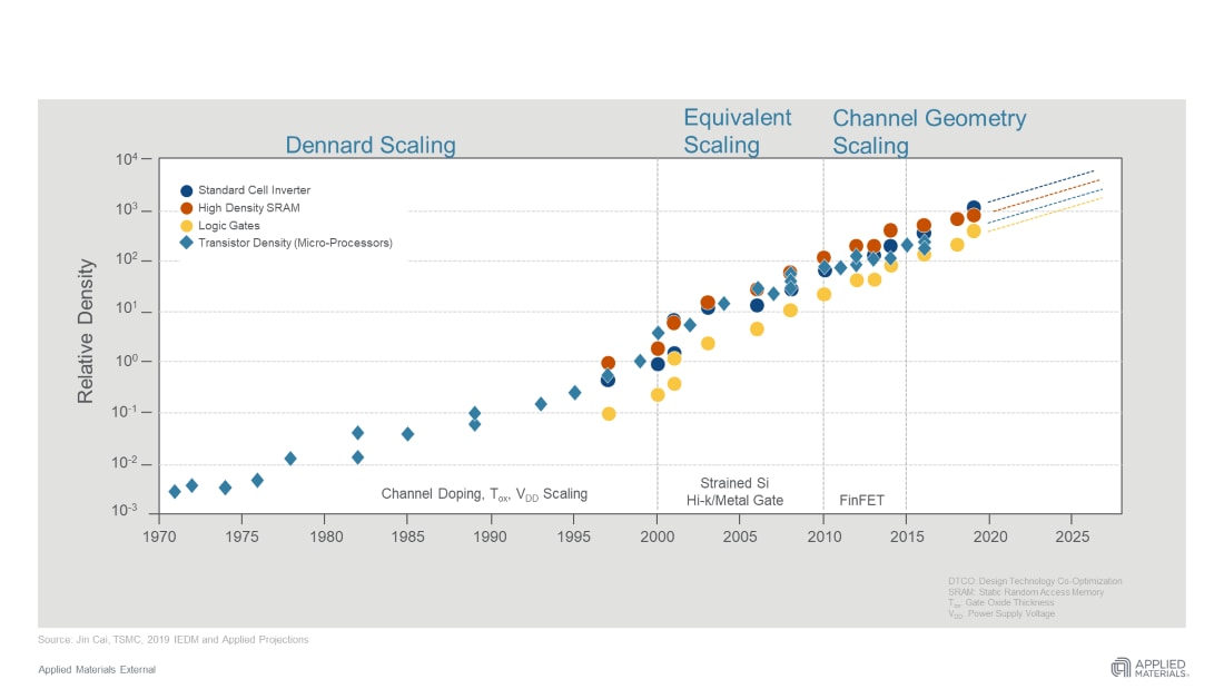
Between 2000 and 2010, gate length and gate oxide scaling hit limits: we could pattern smaller features, but not without physics issues like gate leakage and contact resistance that negated the performance and power benefits of reducing area-cost. We transitioned to “equivalent scaling” whereby the gate length remained at around 30nm and physical gate oxide scaling stalled. Node names were no longer tied to actual dimensions. Instead, using materials engineering techniques such as strained silicon and high-K metal gates, we enabled “PP” benefits to continue even as “AC” scaling slowed. From 2010 onwards, the 3D FinFET architecture arrived to enable further progress in both PP and AC.
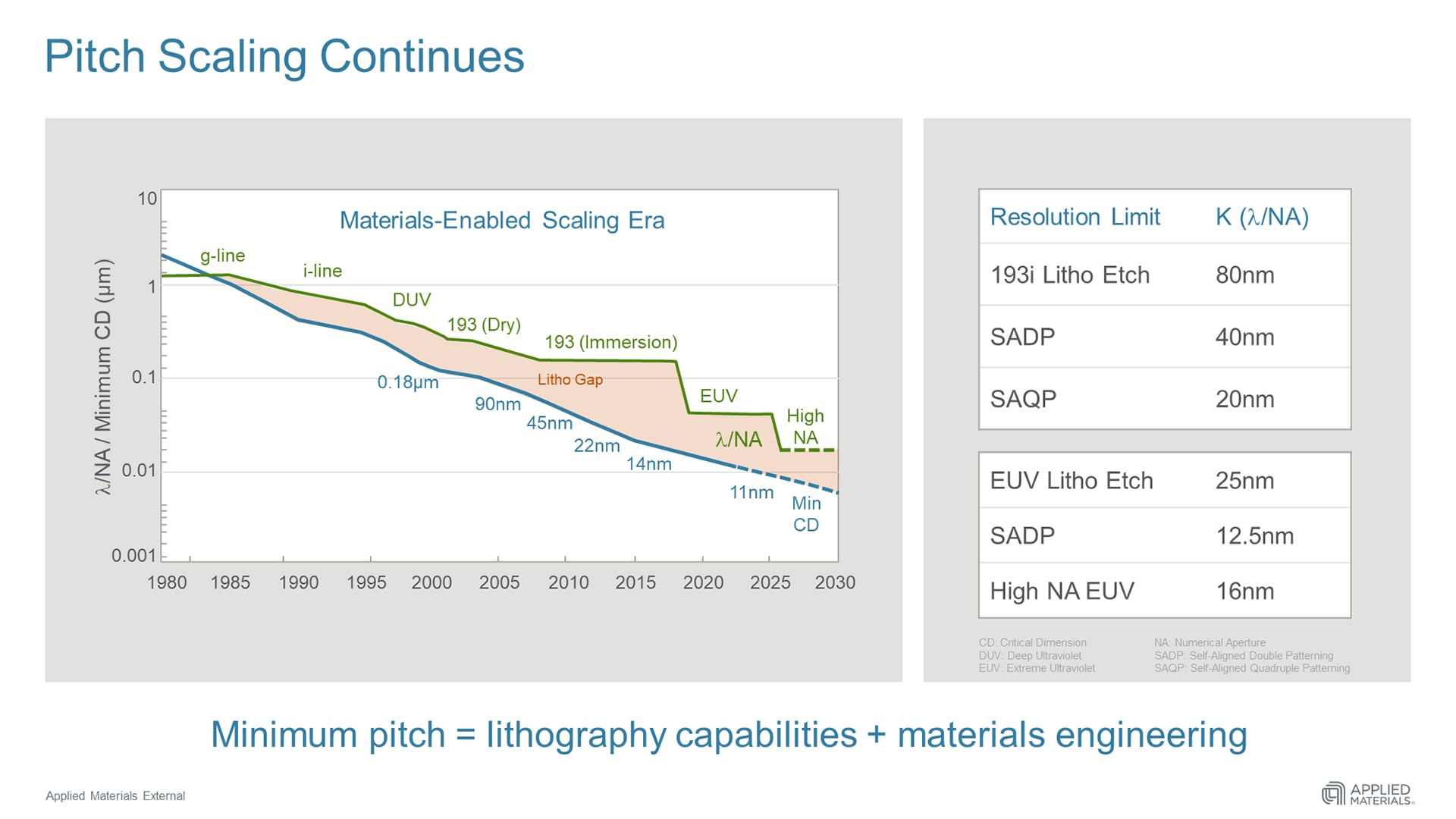
Materials engineering also helped when lithography stalled at 193nm immersion—limiting single-pass patterning to around the 80nm pitch. Double patterning and quad patterning enabled further scaling to the 40nm and 20nm pitch, respectively.
EUV Simplifies Patterning but Complicates Wiring
EUV arrived in time for the 5nm node, enabling 25nm pitch patterning in a single step. However, new materials engineering techniques were required to make EUV practical. For example, transistor contact vias patterned at the resolution limits of EUV are challenging to fill with metal using traditional liner-barrier and fill methods: the area remaining for the metal wiring is so small that contact resistance grows exponentially. Integrated Materials Solutions have enabled selective deposition of contacts, eliminating liner-barriers and producing wide, low-resistance contacts.
New Ways to Shrink
Are there new ways to shrink even further? Yes, in fact, there are two.

As one of our major customers has discussed, continued intrinsic scaling—i.e. classic 2D Moore’s Law—delivers about half of the logic density improvement of the 3nm node. The other half comes from design technology cooptimization—DTCO—which refers to clever rearrangements of the elements of the logic cell to reduce cell area at a constant lithographic pitch.
At our April 21 Master Class, I’ll discuss how we can further scale using EUV—if we can solve the growing materials engineering and metrology challenges I’ll describe in a moment. At our May 26* Master Class, we’ll provide the engineering details of Backside Power Distribution Networks, an innovative, emerging DTCO technique that increases logic density independent of lithography pitch.
Materials Engineering Challenges to Further EUV Scaling
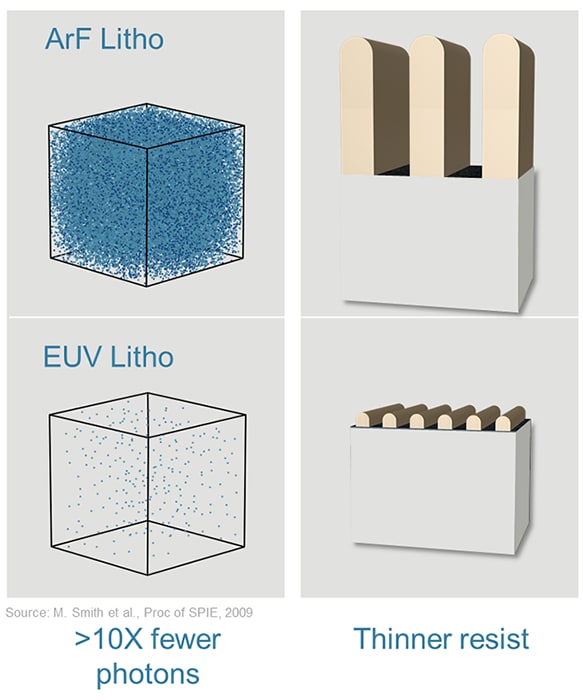
Producing photons using EUV technology is challenging and expensive. As a result, we need to make EUV lithography work using 10X fewer photons than with deep UV. Also, the patterns we make with EUV—such as alternating lines and spaces—are much narrower. As a result, EUV photoresists are much thinner. The thinness enables us to develop the photo mask patterns with fewer photons—and helps prevent the narrow patterns from collapsing into one another.
Issue 1: Correcting Stochastic Errors in EUV Photoresists
In fact, because the photon count and resist thickness is limited, we encounter “stochastic errors” which are imperfections in the lines and spaces we are patterning into the photoresist. The smaller the EUV patterns, the larger the stochastic errors become as a proportion of the device features. If these irregularities are transferred to the wafer, they can result in patterning failures—such as gaps in lines that cause open circuits; bridges between adjacent lines that cause shorts; and misalignment of features in adjacent layers of the chip—called edge placement errors—that reduce yield.
What we need is a materials engineering breakthrough that can manipulate EUV photoresist patterns to heal the stochastic errors and prevent them from being transferred to the wafer.
Issue 2: Reducing EUV Patterning Cost
Chip designers already want to make patterns that are even tighter than the resolution limits of EUV. Designers can divide tight patterns in two so that half the pattern is deposited using a first EUV pass and the other half is deposited in a second step. But the extra EUV step adds considerable cost. What we need is a new technology that can gently extend EUV patterns on the photoresist to create impossibly tight spacing following a single EUV pass.
Issue 3: Increasing the Precision of EUV Patterning Films
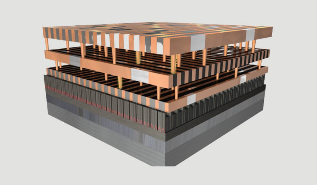
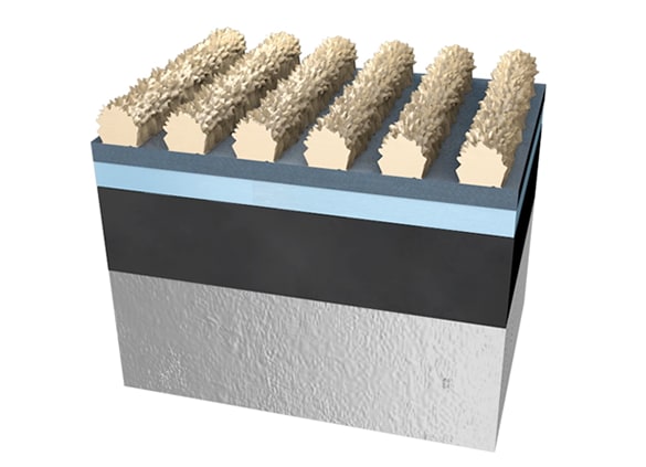
I explained that the EUV photoresist is very thin and delicate. As a result, we need to deposit multiple layers of material between the photoresist and the wafer before etching the intended pattern:
A transfer layer receives the pattern from the EUV photomask—quickly, before the etching fully erodes the photoresist. Below the transfer layer is a hardmask: it receives the pattern and is more resilient, withstanding the longer etch times needed to replicate the pattern in the wafer. There can actually be more than one hardmask layer.
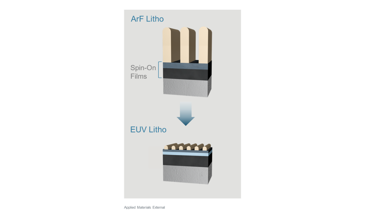
Traditionally, spin-on deposition and films are used to form the transfer layer and hardmask. The films start as a liquid and are inherently soft. Spin-on deposition also has uniformity challenges. Continued EUV scaling calls for a new approach.
Issue 4: Ensuring Photoresist Pattern Fidelity Before We Etch Wafers
Optical overlay tools are used to center the EUV patterns over the wafer before we commit to etching. eBeam CD SEM tools are used to supplement the centering and—importantly—measure the critical dimensions of the photoresist patterns before we etch them into the wafer. Traditional CD SEM eBeam energies can alter the photoresist, potentially distorting the patterns. Traditional CD SEM image resolution has difficulty discerning ever-finer EUV patterns. My colleagues in our eBeam metrology division are working on a new system to address these challenges.
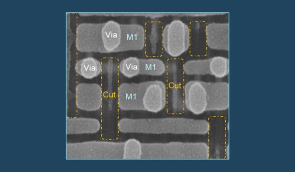
Issue 5: Solving Edge Placement Errors
Chips are made one layer at a time. Each layer can contain billions of individual features—such as lines, line segments and vias. The edges of each of these features need to be properly aligned with their opposite features on the layers above and below. If the features are misaligned, there can be subtle errors that affect power and performance—or significant errors that can ruin entire wafers or a significant percentage of the chips on each wafer. The resulting time-to-market and yield issues are increasingly difficult to solve as we continue to shrink with EUV.
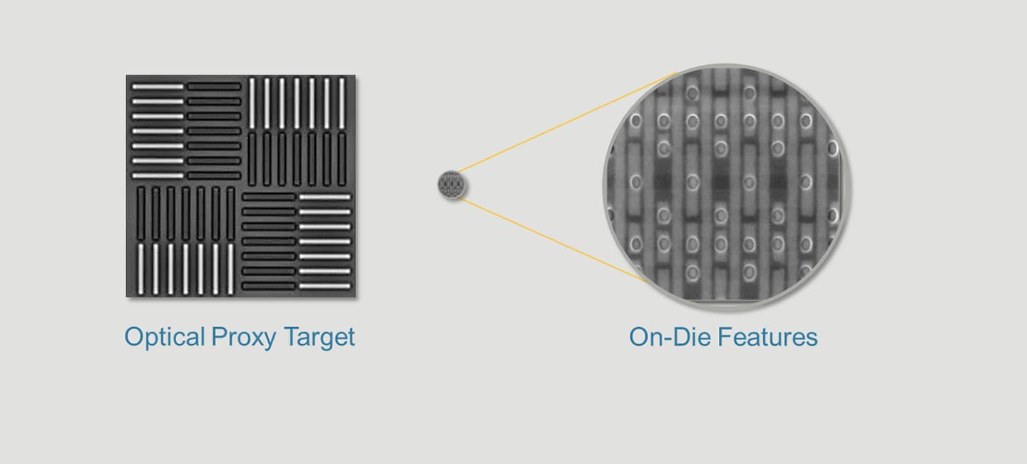
Traditional optical overlay aligns the various layers using “proxy targets” that are placed in non-active areas of the wafer—such as the scribe lines between chips which are sawed away during die singulation. In theory, lining up these marks, one layer at a time, properly aligns all of the billions of feature edges across all of the critical layers of the chip.
In practice, the individual features we are trying to align are at least 10X smaller than the proxy targets. Also, the subtle variability inherent in lithography along with process steps like deposition and etch create subtle issues—such as pitch walking—that cannot be seen and controlled using optical techniques.
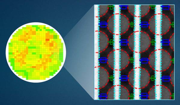
Increasingly, lithography experts are using eBeam technology to scan each 2D layer and identify patterning variations. However, their efforts are still largely focused on diagnosing issues one 2D layer at a time—and making optical adjustments when the next layer of the chip is scanned. As we continue to scale using EUV, engineers are encountering more “blind spots”: they do everything possible using optical corrections and still wind up with edge placement errors that they cannot resolve. Further, if a patterning excursion crops up during high-volume manufacturing, engineers who rely on proxy target approximation can lose weeks of time and output as they await new masks.
What the industry needs is 3D imaging and patterning control that directly images and measures the critical features across multiple layers of the chip simultaneously to quickly characterize and diagnose all of the sources of edge placement errors, including overlay and alignment; line and cut uniformity; line and cut edge roughness; and pitch walking.
Issue 6: Using Big Data and AI to Accelerate Progress
To speed R&D and the ramp to high-volume production, we would ideally obtain massive data and use advanced analytics to disentangle the various contributors to patterning issues. We would use this data to create optimized process recipes with the widest margins—called process windows—to enable intrinsic scaling with EUV to continue well into the future. I invite you to tune into our Master Class to learn more about how we can use sensors, metrology and analytics to accelerate process R&D, ramp new process technologies faster, and enjoy higher yields over the life of a new process technology. We’ll also address the other five materials engineering and metrology issues I described in this blog.
*Projected date
Tags: EUV, 2D Scaling, Moore's Law, materials engineering, Patterning, eBeam, metrology, DTCO
Regina Freed
Vice President, AIx™ Solutions

Regina Freed has more than 20 years of experience in the semiconductor industry, managing semiconductor process and equipment development for both logic and memory processes, including co-optimization between deposition and etch, lithography, metrology, and defect inspection. At Applied Materials, Regina leads our AIx™ program that enables us and our customers to accelerate development and ramp through Actionable Insights as well as control our processes to deliver improved process windows, enabling customers to scale faster and at lower cost, while optimizing device performance.

Adding Sustainability to the Definition of Fab Performance
To enable a more sustainable semiconductor industry, new fabs must be designed to maximize output while reducing energy consumption and emissions. In this blog post, I examine Applied Materials’ efforts to drive fab sustainability through the process equipment we develop for chipmakers. It all starts with an evolution in the mindset of how these systems are designed.
Innovations in eBeam Metrology Enable a New Playbook for Patterning Control
The patterning challenges of today’s most advanced logic and memory chips can be solved with a new playbook that takes the industry from optical target-based approximation to actual, on-device measurements; limited statistical sampling to massive, across-wafer sampling; and single-layer patterning control to integrative multi-layer control. Applied’s new PROVision® 3E system is designed to enable this new playbook.
Breakthrough in Metrology Needed for Patterning Advanced Logic and Memory Chips
As the semiconductor industry increasingly moves from simple 2D chip designs to complex 3D designs based on multipatterning and EUV, patterning control has reached an inflection point. The optical overlay tools and techniques the semiconductor industry traditionally used to reduce errors are simply not precise enough for today’s leading-edge logic and memory chips.