Products & Technologies
Products & Services
Contact
Products & Services
Products & Technologies
Services
Resources
Contact
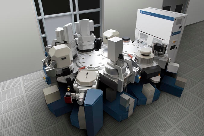
Endura® Volta® W CVD
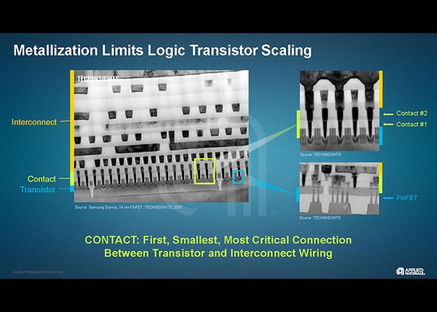
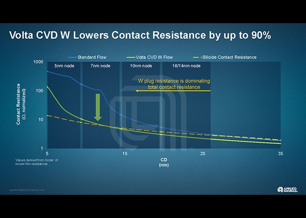
Tungsten has been widely used in logic contact, middle-of-line, and metal gate fill applications for its low resistivity and conformal bulk fill characteristics. Contacts and local interconnects form the critical electrical pathways between the transistors and the rest of the circuit. Hence, low resistivity is crucial for robust and reliable device performance. As scaling has progressed, however, interconnect dimensions have decreased to the point at which contact resistance is becoming an obstacle to realizing optimum transistor performance.
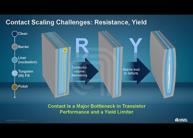
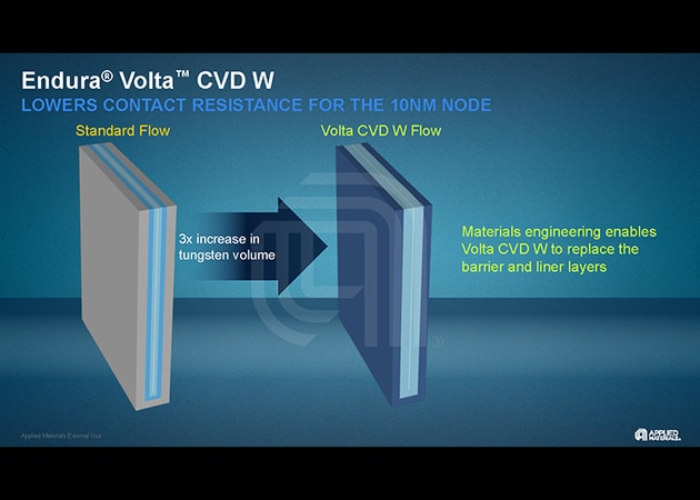
As the cross-section of the interconnect decreases, a growing proportion of the volume is occupied by metal barrier and nucleation layers, leaving less volume for the conducting metal fill. In addition, contact resistance is made worse by each additional metal interface in the plug. The Volta CVD W system relieves these adverse effects through hardware enhancements to the chamber that enable deposition of a W-carbon film using a specialized chemistry. This unique material is capable of serving as both a liner and nucleation layer. It bonds strongly to dielectrics and prevents fluorine diffusion from the subsequent bulk deposition process. Its resistivity is more than 70% lower than that of standard liners (e.g., TiN). Further, as the film is primarily W, it behaves as a nucleation substrate for bulk W. The total thickness of interface films is therefore thinner, enlarging the volume available for low-resistivity W fill.
The Volta CVD W film lowers contact resistance by up to 90%, depending upon critical dimensions and process flow. It thereby improves device power delivery, performance, and efficiency, and extends the W middle-of-line interconnect plug for next-generation devices. This lower resistance also allows for more aggressive scaling at a given node, enabling higher device density.
Click here to learn more.
- 1 / 7
- 2 / 7
- 3 / 7
- 4 / 7
- 5 / 7
- 6 / 7
- 7 / 7