半導體 (Semiconductor)
解決方案與軟體
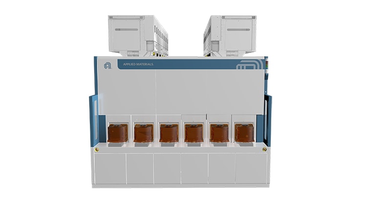
Vistara
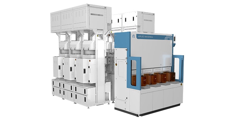
Vistara™ 是一個模組化平台,基於三大特色:靈活性,智慧功能和永續性。Vistara 允許晶片製造商在單一平台上部署最複雜的配方,降低其營運成本,加快營收到位時間並推進永續計劃。
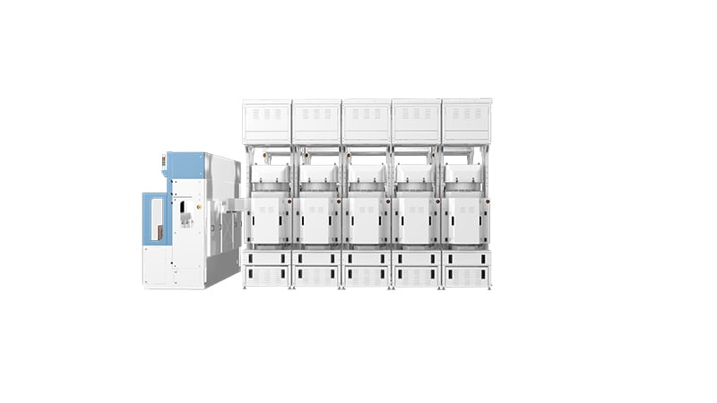
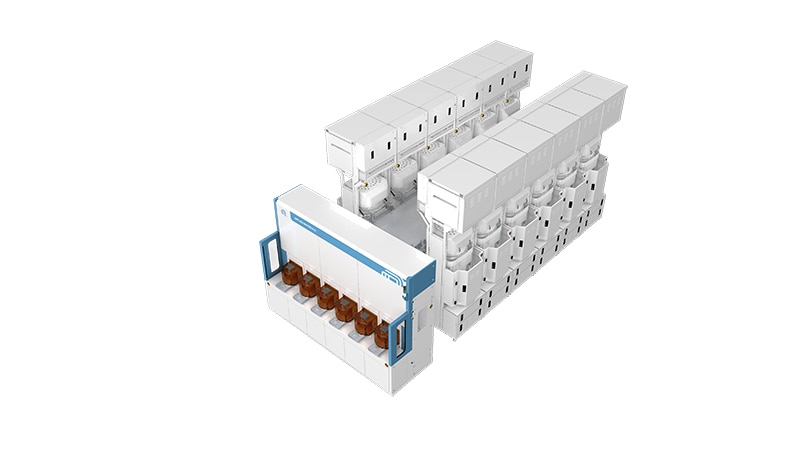
高度靈活的 Vistara 能夠容納應用材料公司和合作夥伴的各種反應室類型、尺寸和配置。它可以配置四或六個晶圓批次裝載埠,以及從最少四個到多達十二個製程反應室。Vistara 既可接受用於原子層沉積和化學氣相沉積等製程的小型反應室,也可以容納用於磊晶和蝕刻等製程的大型反應室。應材與客戶可結合這些反應室,開發整合型材料解決方案 IMS™(Integrated Materials Solution®)配方,從而在真空環境下,於同一系統中完成多個連續晶圓生產製程步驟。
Vistara系統配置了數千個感測器,可將大量數據即時傳送到應材的AIx™軟體平台,該平台涵蓋了研發、製程轉移和擴產、以及大量製造等應用領域。藉由從數千個製程變數所取得的可操作數據,工程師能運用機器學習和人工智慧的強大功能,加速開發製程配方,實現最佳的晶片效能、功率和最大的製程容許範圍。智慧功能應用在整個平台,包括在工廠介面模組中智慧控制負載鎖定,以優化抽氣和排氣時間,幫助晶片製造商減少微粒和缺陷並以最大化良率。平台機器手臂可自動校準,可降低啟動時間達75%。在生產過程中,Vistara 會持續監測和校準其組件,以最小化人工干預,最大化正常運作時間,並預測維修需求。
半導體製程複雜性和步驟增加了生產每片晶圓所需的能源和材料。Vistara 是第一個專為推進應材「3x30」倡議而打造的平台,旨在 2030 年之前將同等能源使用量、化學品使用量、以及無塵室佔地面積需求減少30%。工程師優化了該平台對能源密集型附屬製造區組件的使用方式,包括泵浦,熱交換器和冷卻系統,並重新設計了 Vistara 的氣體控制板。與之前的平台相比,這些改進可以將平台的能源消耗降低達 35%,幫助晶片製造商減少其在範疇1和範疇2的碳排放。Vistara 還可以將系統的無塵室佔地面積減少達 30%。
- 1 / 5
- 2 / 5
- 3 / 5
- 4 / 5
- 5 / 5