半导体 (Semiconductor)
解决方案与软件
Vistara
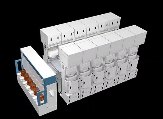
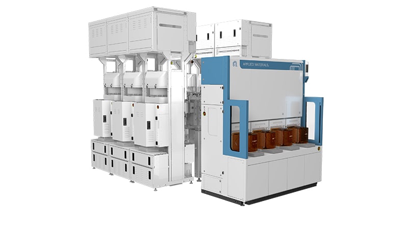
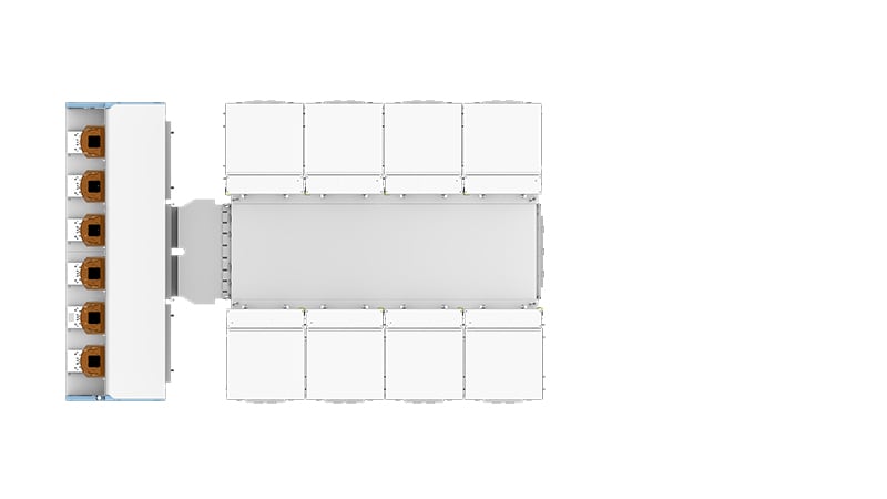
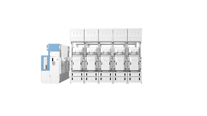
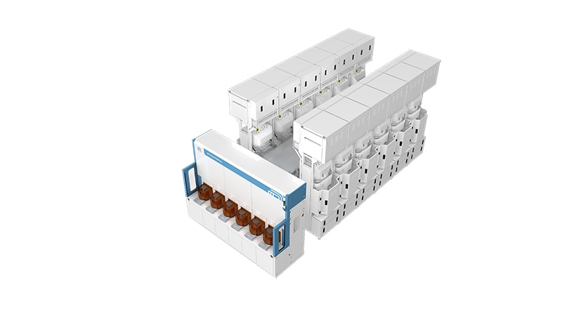
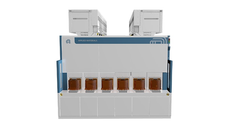
Vistara™ 是一个基于灵活性、智能性和可持续性三个支柱的模块化平台。Vistara允许芯片制造商在单个平台上部署他们极为复杂的配方,降低运营成本,缩短盈利时间,并推进可持续发展。
高度灵活的Vistara能够使用应用材料公司甚至其合作伙伴提供的各种腔室类型、尺寸和配置。它可以配置四个或六个晶圆批处理加载口,从最少四个到多达十二个工艺腔室。Vistara既可接受用于原子层沉积和化学气相沉积等工艺的较小腔室,也可接受用于外延和刻蚀等工艺的较大腔室。应用材料公司及其客户可以将这些腔室组合在一起,开发IMS™(集成材料解决方案™)配方,从而在一台设备的真空环境内完成多道晶圆制造工艺步骤。
Vistara系统配置有数千个个传感器,将大量实时数据传输到应用材料公司的AIx™ 软件平台上,该平台提供研发、工艺转移和爬坡以及大规模量产等应用。来自数千个工艺变量的可操作数据使工程师能够利用机器学习和人工智能的力量来加速配方优化,以实现最佳芯片性能、功耗和最宽的工艺窗口。智能功能贯穿整个平台,包括在工厂接口模块智能控制晶圆装载,以优化腔室抽气和排气时间,帮助芯片制造商减少污染和缺陷,从而最大限度地提高产能。平台机器人会自动校准,将启动时间缩短多达 75%。在生产过程中,Vistara会持续监控和校准其组件,以最小化减少人工干预,最大化正常运行时间并预测保养需求。
半导体工艺复杂性和步骤的增加导致了生产每片晶圆所需能源和材料的增加。Vistara是首个专为推进应用材料公司的 “3x30” 倡议而构建的平台,旨在到2030年在实现同等产出的条件下,节约30%的能源消耗、化学品使用的影响和洁净室占地面积 工程师们优化了平台使用能耗密集型子设备(包括泵、热交换器和制冷机)的方式,并重新设计了Vistara的气柜(供气面板)。与以前的平台相比,这些改进使平台能耗降低了多达35%,有助于芯片制造商降低其范围1和范围2的排放。Vistara还可将系统的洁净室占地面积减少了多达30%。
- 1 / 5
- 2 / 5
- 3 / 5
- 4 / 5
- 5 / 5