Products & Technologies
Products & Services
Contact
Products & Services
Products & Technologies
Services
Resources
Contact
Posted
March 02, 2020

Stay updated on our content.
Bringing AI to the Edge Improves Data Management and Energy Efficiency

Mar 02, 2020
Welcome to the latest in a series of blogs inspired by a fascinating panel discussion during the recent IEEE International Electron Devices Meeting (IEDM). The panel was moderated by my colleague Regina Freed, who was joined by experts from Facebook, IBM Research, Intel, Stanford University and TSMC to explore “The Future of Logic: EUV is Here, Now What?”
A key takeaway from the panel, as Regina noted in her post-event blog, is that emerging applications enabled by AI and Big Data are causing the electronics industry to forge new and divergent paths. This is largely due to the varying set of performance, power and area-cost (PPAC) requirements of the hundreds of billions of smart devices that will comprise the Internet of Things (IoT) in the decade ahead. As my other colleague Kevin Moraes recently wrote in his blog about the panel discussion, addressing these requirements will require the ecosystem to work together in new ways using a combination of technologies—what we at Applied Materials refer to as a “new playbook” for semiconductor design and manufacturing.
I will now take a closer look at another topic raised by the panel: how to solve the scaling challenges of the IoT. First let’s examine the problem, then get into the solutions.
The IoT, in the form that we envision, is a game of staggering numbers: the total connected devices in use by 2030 could range from 500 billion to 1 trillion nodes, potentially generating a volume of raw data exceeding 10s of zettabytes, enough to fill several billions of 10TB hard drives every year on their own (note: 1 ZB = a billion TB). The current node and server model of cloud compute architecture will strain under the load of so much data, in particular the data networks that would be hauling data from the endpoints to central servers where processing occurs. As this use case develops, the industry has been prompted to adapt new types of nonvolatile memory, intended to succeed DRAM or NAND flash standalone memory products, into embedded memories fabricated on the die using a logic process.
Panelist Ali Keshavarzi, Adjunct Professor in the Electrical Engineering Department of Stanford University, observed that at a time of this burgeoning demand for intelligent sensor-driven IoT devices, two mainstays of the semiconductor industry—classic Moore’s Law scaling and the Von Neumann computing architecture—are running out of steam. To make the vision of a trillion IoT devices a reality, a major leap in energy efficient computing is needed.
“The situation today is that you sense the data, send the raw bits to a central cloud location, process that data in the cloud, and then a decision comes back down that causes an action,” said Ali. “Clearly, this is not scalable, because there's going to be way too much data and the energy needed to transmit this data at nanojoules/bit to the cloud is simply not available at the edge. On top of that, many of the new applications require latency that is incompatible with sending data back and forth to the cloud.”
The panelists also predicted that the market inflection of intelligent edge products could extend to areas beyond architectural solutions towards energy efficiency.
“The requirements for extremely low power and high performance are clearly divergent, and the materials challenges for these are very different,” said panelist Bala Haran, Master Inventor and Director of Silicon Process Research at IBM Research. “If you look at the periodic table, there are about 67 usable elements for semiconductor manufacturing, and we are using about 50 percent of them today. If you project out over the next decade, we can expect that number to increase to about 70 percent. So new elements are definitely going to come into play, whether it's new dopants for epitaxy, new precursors or pure new elements in the back end.”
Ali added that IoT platforms using conventional computing designs have a built-in problem with data latency that is unable to adequately serve applications requiring a real-time response—for example, managing energy utility data during times of peak load or handling video-processing to control a microdrone. Energy consumption and the need for data security at the edge are only compounding the limitations of today’s IoT devices.
“I think a path forward is to develop capabilities that enable edge intelligence such that we take computing locally to the endpoint device and reduce the data bits into information bits that are more valuable before going to the cloud,” said Ali. “I'm not saying that we are replacing the cloud. What we're going to do is better regulate the flow of the information by processing it locally.”
Ali calls this solution Edge Intelligence: the approach where the data is processed at the point of data collection enabling autonomy in decision making and autonomy in energy use.
Add the fact that IoT applications are increasingly adopting AI algorithms, and the performance and power delta worsens. Ali proposed a scenario in which AI reinforcement learning is used to train a device using a deep neural network. Because not all layers of the network are constantly changing, all static data can be stored locally at the edge using embedded memory, while all data that is in flux can be stored to SRAM.
In a follow-on conversation, Ali called on the industry to adopt new technology platforms to help move AI-based intelligent data processing more efficiently to the edge. A critical component is the use of ferroelectric memory, a form of embedded nonvolatile memory that is CMOS compatible. Superior energy efficiency (potentially up to a 100x improvement) is possible by using this femtojoule/bit memory in a non-Von Neumann architecture and minimizing unnecessary data movement with devices based on memory-centric compute.
“Ferroelectric memory can provide a level of energy efficiency in devices that has not been seen before, enabling these edge devices to operate in the energy-starved edge environment,” said Ali. “This new processor architecture combined with new algorithms will lead to orders of magnitude improvements in performance per watt. These future data-flow architectures implemented in a memory-centric computing technology can even enable learning capabilities in the field for intelligent IoT devices. Think of it as ‘small system AI at the edge’.”
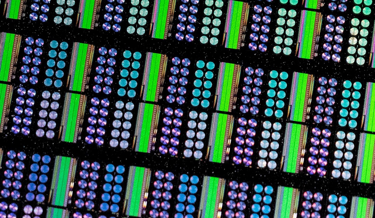
Another type of memory that is emerging as a leading candidate for storing IoT device software and AI algorithms is MRAM (magnetic random access memory), which has been in design for years and is now reaching the cusp of practical volume manufacturing. For IoT devices, MRAM provides fast, low-power, nonvolatile memory with high endurance. Applied Materials is helping accelerate the availability of MRAM with our Endura® Clover™ PVD platform. This integrated materials solution allows the novel materials used in MRAM to be deposited with atomic-level precision at an industrial scale. In turn, this lets IoT designers place large amounts of fast memory closer to their compute resources to achieve desired performance and power-efficiency targets. This closer proximity can address the performance bottleneck issues and reduce power by shortening the space between where data resides and the raw compute engines.
The Endura Clover platform is among the systems now available at our recently opened Materials Engineering Technology Accelerator (META Center). The META Center is a unique collaboration facility that provides the industry with a pilot manufacturing environment where new AI chip designs can be validated before being transferred to customer high-volume fabs.
By helping the industry develop new chip architectures that move memory closer to compute, we can enable more intelligent edge devices and more efficient processing of data. This is important when one considers the energy implications of all the sensors and smart devices that will be in use throughout the world in the years ahead.
Stay tuned for more from the IEDM panel as our next post will explore the role of advanced packaging and heterogenous design in driving PPAC improvements.
Tags: IEDM, logic, AI, Big Data, Edge Intelligence, cloud computing, new materials, augmented reality, New Playbook, Moore’s Law, iot, MRAM, EUV, META Center

Michael Stewart
Now is the Time for Flat Optics
For many centuries, optical technologies have utilized the same principles and components to bend and manipulate light. Now, another strategy to control light—metasurface optics or flat optics—is moving out of academic labs and heading toward commercial viability.
Seeing a Bright Future for Flat Optics
We are at the beginning of a new technological era for the field of optics. To accelerate the commercialization of Flat Optics, a larger collaborative effort is needed to scale the technology and deliver its full benefits to a wide range of applications.
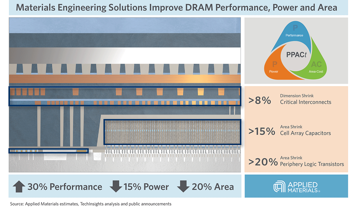
Introducing Breakthroughs in Materials Engineering for DRAM Scaling
To help the industry meet global demand for more affordable, high-performance memory, Applied Materials today introduced solutions that support three levers of DRAM scaling.