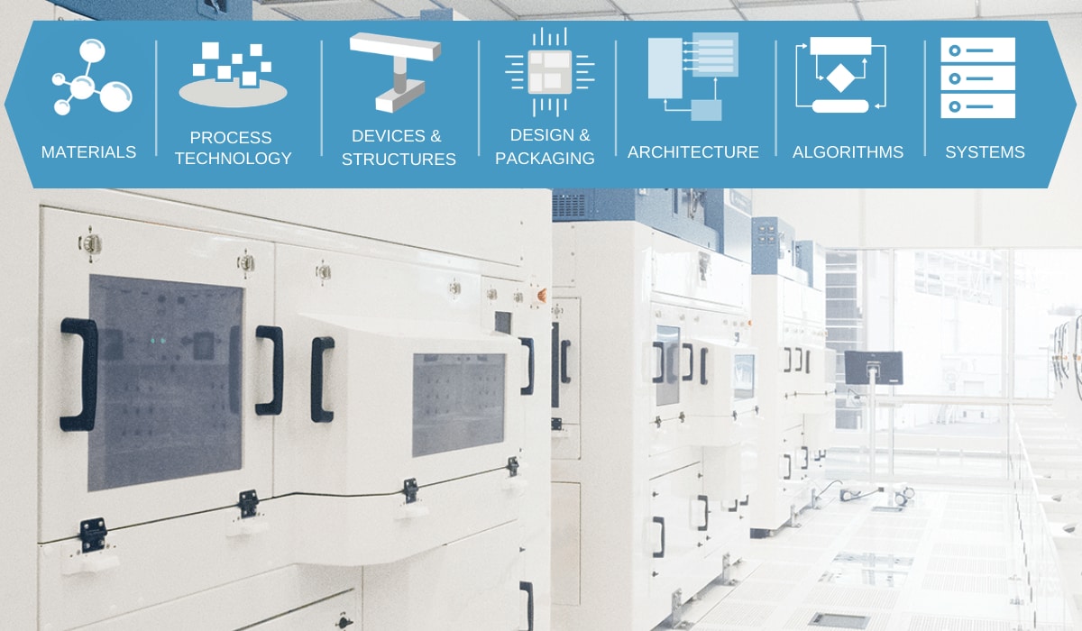
Products & Technologies
Products & Services
Contact
Products & Services
Products & Technologies
Services
Resources
Contact
Posted
November 08, 2019

Stay updated on our content.
Enabling the AI Era of Computing – Part 3
Nov 08, 2019
This is the third in our three-part series describing how the computing industry can collaborate on a “New Playbook” for innovation to enable the AI Era. Part one outlined the what: the major opportunities and technology challenges facing society as we enter the third decade of the 21st century. Part two gave us the how: codesign, whereby engineers from a variety of disciplines collaborate to find uncommon solutions to big challenges. The blog highlighted the need for parallel development of “simulation proof of concepts” and “physical proof of concepts”—and identified the need for a state-of-the-art cleanroom facility where codesigned AI innovations can be piloted before being transferred to customer high-volume fabs.
Here in part three, I’ll add the where: where we can test codesigned chip innovations for the AI Era—to accelerate the future of computing, from materials to systems. The answer is: our new Materials Engineering Technology Accelerator (META Center), which—I’m delighted to announce—is now open for collaboration.
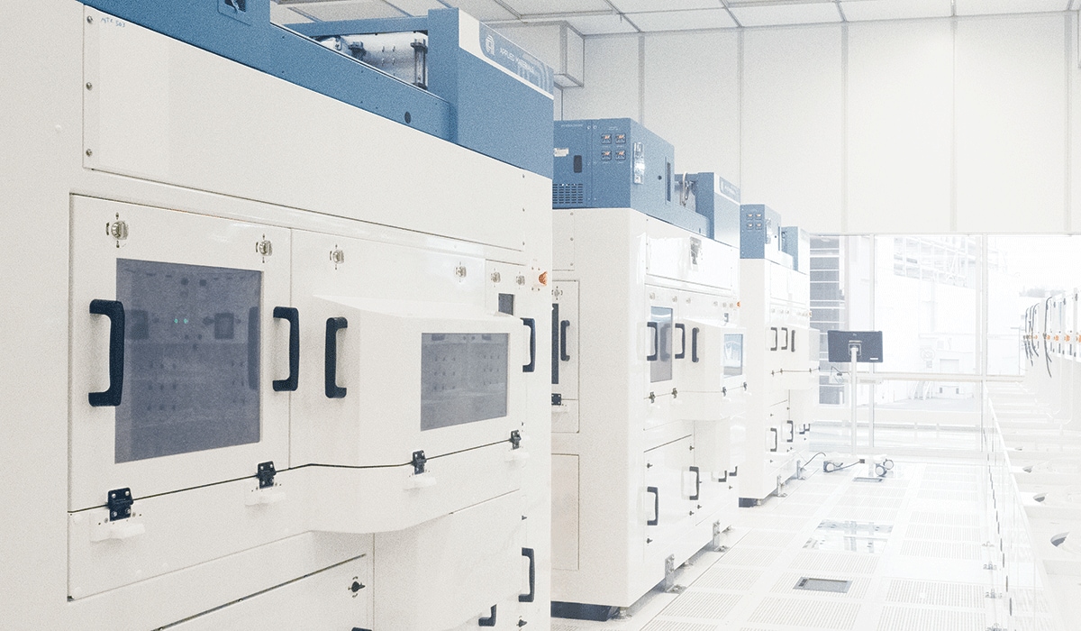
Located at the State University of New York Polytechnic Institute (SUNY Poly) campus in Albany, New York, the META Center is a unique facility aimed at speeding the prototyping of new chip materials, process technologies and devices. It’s a state-of-the-art cleanroom where new ideas can be validated in a pilot manufacturing environment with input from innovators across the AI ecosystem, from materials engineers to system designers. In effect, it is the physical embodiment of the codesign concept. The META Center represents one of the critical elements of the New Playbook, providing the industry with a place to test physical proof of concepts for new AI chip solutions—and bring AI Era ideas to reality. In short, to accelerate “lab to fab.”
One of the first projects currently running in the center is a new type of memory targeting Internet of Things devices that need low-power, nonvolatile, high-density code and data storage. Applied’s recently launched Endura® Clover™ MRAM PVD platform is among the systems now available at the META Center.
Applied Materials and the META Center are open to—and for—collaboration. Please join us in the spirit of codesign, being open-minded to the ideas that exist outside of our immediate specialties. And being willing to expand and adapt our vocabularies to get to a common understanding of the technical challenges we can solve to accelerate innovation, from materials to systems.
The META Center is the latest addition to Applied’s worldwide, collaborative R&D platform. These include the Maydan Technology Center in Silicon Valley, our 300mm development fab where chipmakers work shoulder to shoulder with Applied engineers to prove the capabilities of new chipmaking systems and recipes. Singapore is home to the Advanced Materials Lab, established in conjunction with the National University of Singapore, where we engineer novel materials and the methods for integrating materials into new process technologies. Also in Singapore is our Advanced Packaging Lab, a pilot wafer-level packaging facility aimed at developing new ways to combine memories for higher density as well as encapsulate heterogeneous logic designs in high-performance substrates.
Together, these labs constitute an open innovation platform where engineers from established and emerging fields can join us in conceiving, developing and piloting the technologies that shape the future.
Tags: AI, artificial intelligence, materials engineering, computing, Codesign, AI Design Forum, Moore's Law, chip design, machine learning, META Center, Collaboration, r&d, New Playbook

Steve Ghanayem
Now is the Time for Flat Optics
For many centuries, optical technologies have utilized the same principles and components to bend and manipulate light. Now, another strategy to control light—metasurface optics or flat optics—is moving out of academic labs and heading toward commercial viability.

Seeing a Bright Future for Flat Optics
We are at the beginning of a new technological era for the field of optics. To accelerate the commercialization of Flat Optics, a larger collaborative effort is needed to scale the technology and deliver its full benefits to a wide range of applications.
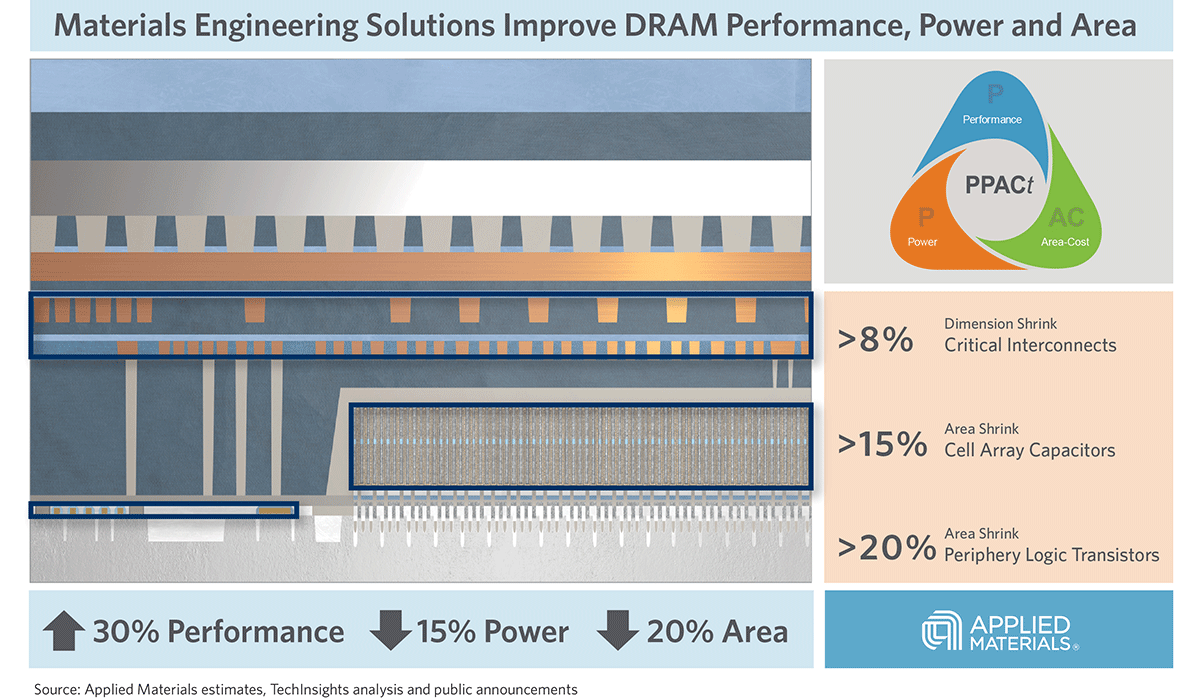
Introducing Breakthroughs in Materials Engineering for DRAM Scaling
To help the industry meet global demand for more affordable, high-performance memory, Applied Materials today introduced solutions that support three levers of DRAM scaling.