Products & Technologies
Products & Services
Contact
Products & Services
Products & Technologies
Services
Resources
Contact
Posted
July 09, 2019

Stay updated on our content.
Accelerating New Memory Technologies for the Internet of Things and Cloud Computing
by Kevin Moraes
Jul 09, 2019
At Applied Materials, our labs and conference rooms are filled with scientists and engineers. Our people are inspired to be the first to solve the most complex materials engineering challenges—to make possible the products that change the world.
Traditionally, these challenges revolved around very specific semiconductor physics questions posed by our customers and answered by breakthroughs initially measured in microns and nanometers—and now in angstroms. Today, at the beginning of the AI and Big Data Era, we are working to support our customers and the industry downstream to address bigger questions:
- How can we more efficiently collect, process, store and analyze the mountains of data AI requires?
- What types of computing architectures can best deliver the performance, power efficiency and cost requirements of the tens of billions of devices that will create the Internet of Things?
- How can we further optimize chips for machine learning and inferencing applications in cloud data centers and edge devices?
- What does the complete solution look like—from materials to systems?
You might expect these questions to be asked further along the technology hierarchy. However, a materials engineering leader like Applied now must ask them as well. We won’t allow the growth potential of the AI Era of computing to be constrained by the slowing of Moore’s Law scaling. We will instead enable a new playbook for semiconductor design and manufacturing.
This strategy underpins our launch today of new high-volume manufacturing systems for emerging memories aimed at the Internet of Things and cloud computing. As my colleagues have explained in recent blogs, the AI Era is driving innovations in memory technology. A key part of this is to put large amounts of fast memory closer to compute resources to achieve desired performance and power-efficiency targets. Closer proximity can address the performance bottleneck issues and reduce power by shortening the space between where data resides and the raw compute engines. This reduces latency and the energy required to shift vast data sets back and forth between memory and compute. Three memories in particular—MRAM, ReRAM and PCRAM—show promise as leading candidates to bring performance, power and cost benefits to IoT devices and cloud computing servers, but all of them are based on new materials that have been too challenging for high-volume manufacturing…until today.
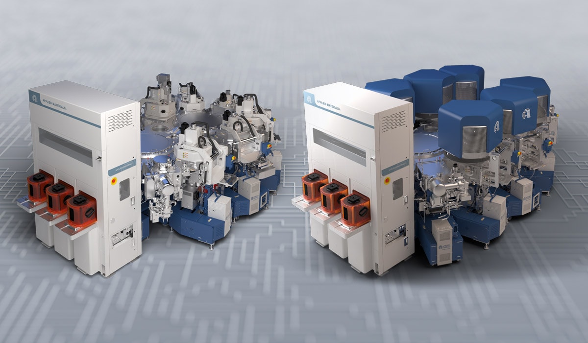
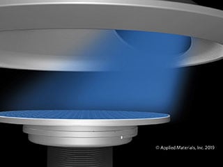
Applied’s new Endura® Clover™ PVD platform for MRAM and Endura® Impulse™ PVD platform for PCRAM and ReRAM are the most sophisticated chip-making systems the company has ever developed. These new, integrated materials solutions allow the novel materials used in MRAM, ReRAM and PCRAM to be deposited with atomic-level precision at an industrial scale. They are like a factory within a machine.
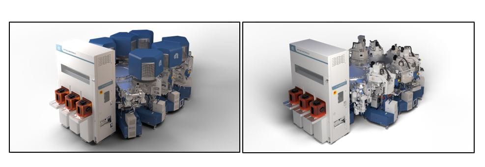
The Applied Endura® Clover™ PVD platform for MRAM (left) and Endura® Impulse™ PVD platform for PCRAM and ReRAM (right) are the most sophisticated chip-making systems Applied has ever developed.
MRAM is emerging as a leading candidate for IoT devices because it is low power, nonvolatile, relatively fast and offers high endurance. It’s based on a magnetic tunnel junction (MTJ), a component that consists of two magnetic layers separated by an insulating layer. Think of it as taking a read/write head from a hard disk drive and shrinking it down to a nanoscale and producing billions of them on a chip. An MRAM stack includes over 30 layers of materials that must be precisely deposited while ensuring distinct, precise interfaces. Attributes such as thickness must be tightly controlled and measured. All of this must be done in an ultra-tight vacuum without exposing the sensitive materials to the impurities of the atmosphere.
An MRAM stack includes over 30 layers of materials that must be precisely deposited while ensuring distinct, precise interfaces.
PCRAM and ReRAM are fast, nonvolatile, low-power, high-density memories that can be used as storage class memory to fill the widening price-performance gap between server DRAM and storage. PCRAM is based on “phase change” materials—similar to those used in DVD disks—that transition from highly amorphous material arrangements to crystalline arrangements with heat as the programming mechanism. ReRAM is made using new materials that act like a fuse. Programming is done by applying electric current to the resistive materials and reading is done by sensing different levels of resistance. Both PCRAM and ReRAM are made using composite materials (consisting of three or more different elements combined) that are highly susceptible to impurities.
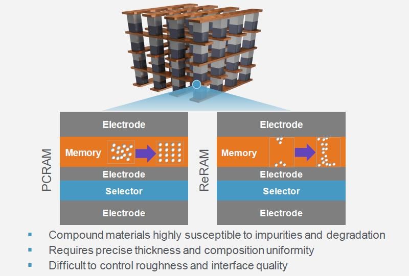
Manufacturing challenges of PCRAM and ReRAM.
To enable the high-volume production of MRAM, PCRAM and ReRAM, Applied’s systems introduced today deliver several breakthroughs in materials engineering to create new films and structures that previously were not possible. For MRAM, we developed a multi-cathode PVD chamber that can very precisely deposit ultra-thin layers of five different materials with extreme uniformity and very low energy to prevent unwanted intermixing of the materials.
For MRAM, Applied Materials developed a multi-cathode PVD chamber that can very precisely deposit ultra-thin layers of five different materials with extreme uniformity and very low energy to prevent unwanted intermixing of the materials.
The Clover MRAM PVD platform also integrates pre-cleaning, cryonic cooling and high-temperature thermal treatments—along with on-board metrology (more on that below)—all under the highest level of vacuum ever achieved in an Applied system. For PCRAM and ReRAM, the Endura Impulse PVD platform consists of up to nine process chambers integrated under vacuum along with on-board metrology to allow the precise deposition and control of the multi-component materials used in these memories, which is essential to achieving high performance, reliability and endurance—at an industrial scale.
Perhaps the most exciting breakthrough we are providing in our new systems is on-board metrology. This capability is critical to achieving layer-to-layer thickness control and enabling faster ramp time and better production yield. This is essential for all three emerging memory types, but especially for MRAM where some of the layers must be only 8-12 atoms high, with film uniformity variances of less than the height of a single atom! Ensuring film uniformity is critical to both read performance and endurance. Conventional metrology techniques require moving the wafer in and out of the deposition system—thereby breaking vacuum and damaging the sensitive materials. With on-board metrology, we are putting “eyes” in the system to measure and monitor the thickness of the MRAM, PCRAM and ReRAM layers with sub-angstrom sensitivity—as they are created—to ensure atomic-level uniformity without risk of exposure to the outside environment.
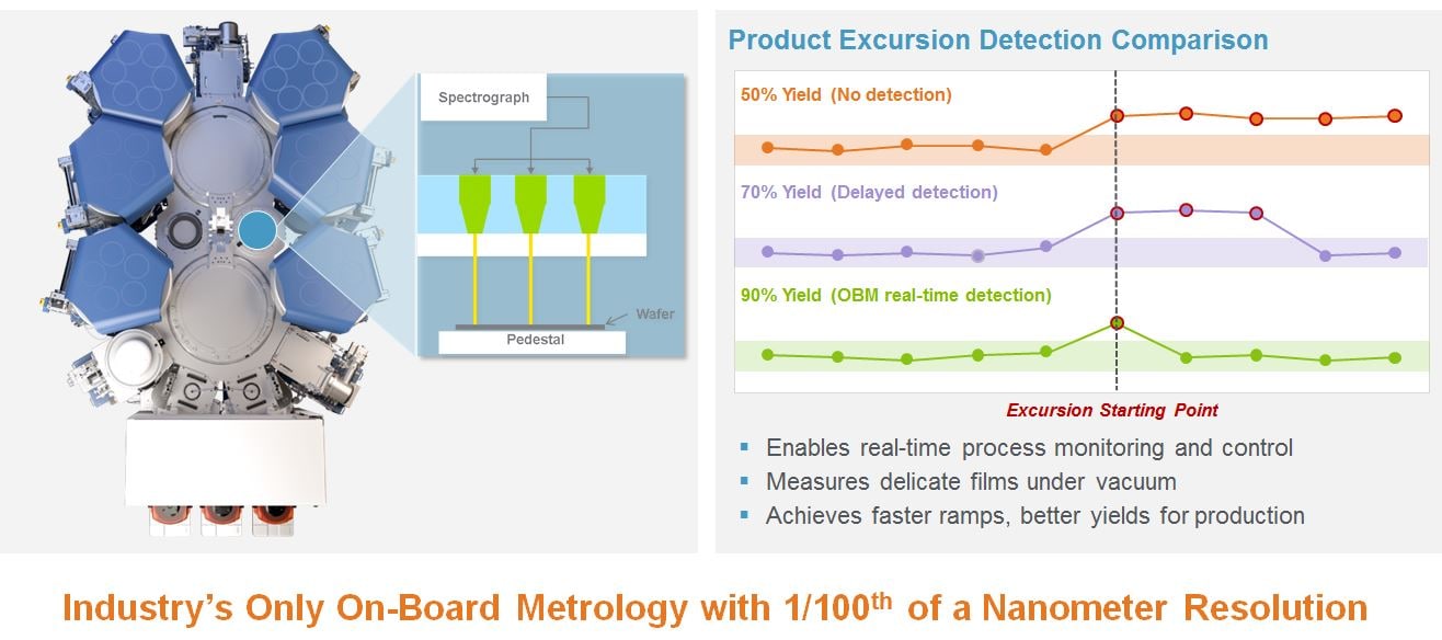
On-board metrology enables precise thickness control.
As the industry moves forward in the AI Era of computing, there will be increasing interest in new types of memory along with continued advancements in conventional memories. Key to all these efforts is the use of new materials and 3D structures to achieve improvements in chip performance, power and cost. This is what we are enabling with our new integrated materials solutions for MRAM, PCRAM and ReRAM—solving complex technical challenges to enable innovative computing solutions at industrial scale.
Tags: AI Era, MRAM, ReRAM, PCRAM, Big Data, iot, cloud computing
Kevin Moraes
Corporate Vice President, Strategy and Marketing, Semiconductor Products Group

Dr. Kevin Moraes serves as Corporate Vice President of Strategy and Marketing at Applied Materials, leading global initiatives that drive growth across key semiconductor segments. In this role, he aligns market insights with business priorities, shapes competitive positioning, and enables customer success through technology inflections. Previously, he held leadership positions in product management and technology development within the company. He earned a Ph.D. in materials science and engineering from Rensselaer Polytechnic Institute, an MBA from the University of California, Berkeley, and a bachelor’s degree in chemical engineering from Annamalai University.
Now is the Time for Flat Optics
For many centuries, optical technologies have utilized the same principles and components to bend and manipulate light. Now, another strategy to control light—metasurface optics or flat optics—is moving out of academic labs and heading toward commercial viability.
Seeing a Bright Future for Flat Optics
We are at the beginning of a new technological era for the field of optics. To accelerate the commercialization of Flat Optics, a larger collaborative effort is needed to scale the technology and deliver its full benefits to a wide range of applications.
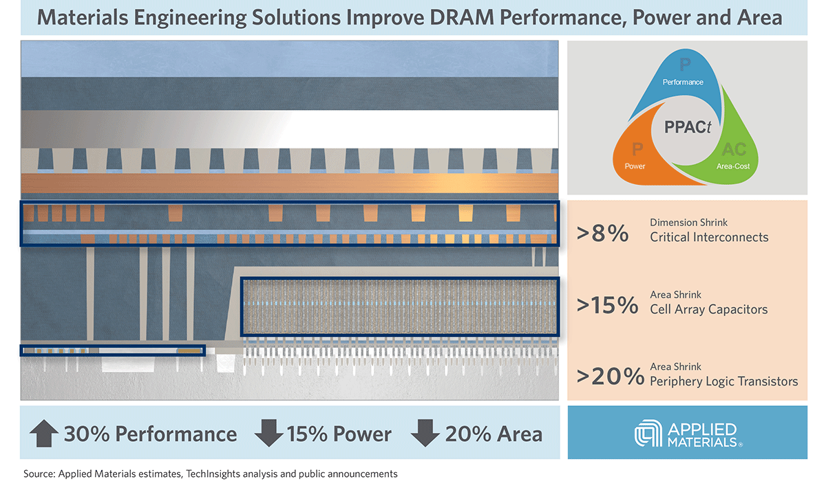
Introducing Breakthroughs in Materials Engineering for DRAM Scaling
To help the industry meet global demand for more affordable, high-performance memory, Applied Materials today introduced solutions that support three levers of DRAM scaling.