Products & Technologies
Products & Services
Contact
Products & Services
Products & Technologies
Services
Resources
Contact
Posted
May 06, 2019

Stay updated on our content.
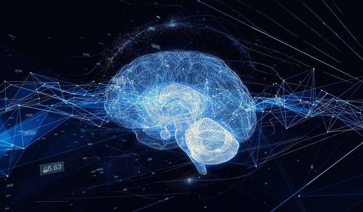
The AI Era is Driving Innovations in Memory
May 06, 2019
Industries from transportation and healthcare to retail and entertainment will be transformed by the Internet of Things, Big Data and Artificial Intelligence (AI), which Applied Materials collectively calls the AI Era of Computing.
The previous computing eras—Mainframe/Minicomputer, PC/Server and Smartphone/Tablet—all benefitted from advances in Moore’s Law whereby 2D scaling was accompanied by simultaneous improvements in performance, power and area/cost—also called “PPAC.”
While AI Era applications are booming, Moore’s Law is slowing; as a result, the industry needs breakthroughs beyond 2D scaling to drive PPAC in new ways. Specifically, we need new computing architectures, new materials, new structures—especially area-saving 3D structures—and advanced packaging for die stacking and heterogeneous designs.
AI Era architectural changes are influencing both logic and memory. Machine learning algorithms make heavy use of matrix multiplication operations that are cumbersome in general-purpose logic, and this is driving a move to accelerators and their memories. AI compute includes two distinct memory tasks: first, storing the intermediate results of calculations; and second, storing the weights associated with trained models.
Performance and power are important in the cloud and in the edge, and innovations in memory can help. One approach using existing memory technologies is “near memories” whereby large amounts of working memory are condensed, placed in close physical proximity to logic, and connected via high-speed interfaces. As examples, 3D stacking and through-silicon vias are gaining traction. One major drawback of SRAM and DRAM as “working memories” in these applications is that they are volatile and need a constant supply of power to retain data—such as weights.
To reduce power in the cloud and edge, designers are evaluating new memories that combine high performance with non-volatility so that power is only needed during active read and write operations. Three of the leading new memory candidates are magnetic random-access memory (MRAM), phase-change RAM (PCRAM) and resistive RAM (ReRAM).
Instead of using electrical charges, all three employ new materials that can be engineered to create high and low states of resistivity which in turn represent zeroes and ones. MRAM uses changes in magnetic direction to control resistivity. PCRAM uses changes in the arrangement of a material, from amorphous to crystalline. ReRAM creates a filament within a material. Both PCRAM and ReRAM offer the possibility of intermediate stages of resistivity that can allow multiple bits to be stored in each cell.
Let’s examine AI Era computing applications and how they are driving innovations in the roadmap.

Figure 1. The AI Era is Driving a Renaissance in Semiconductor Innovation
IoT edge applications can be segmented into low-performance/low-power applications and high-performance/higher-power applications.
Examples of low-performance/low-power applications are security cameras that can employ AI algorithms for applications such as face and speech recognition at the point-of-use. A design goal is to process as much data at the edge as possible and transmit only significant information to the cloud. Performance demands are low because sampling frequency is low. Power consumption—including standby power—is critical, especially in battery-powered devices.
The industry currently uses SRAM memory in edge devices. SRAM is not ideal because it requires as many as six transistors per memory cell, and active leakage power can be high. SRAM is not power-efficient for storing weights, especially in low-frequency designs. As an alternative, MRAM promises several times more transistor density, enabling higher storage densities or smaller die sizes. Another key feature of MRAM is that it can be designed into the back-end interconnect layers of embedded system-on-chip products (SOCs). The MRAM can be used to store the SOC’s operating system and applications, eliminating the need for an embedded flash chip for this purpose, thereby reducing total system chip count and cost.
High-performance “near-edge” applications such as defect detection and medical screening require higher performance. An MRAM variant called spin-orbit-torque MRAM (SOT-MRAM) may prove faster and lower power than spin-torque-transfer MRAM (STT-MRAM).
Cloud computing requires the highest computing performance possible, and training requires enormous amounts of data to be brought close to machine learning accelerators which accordingly have large on-chip SRAM caches supplemented by large, off-chip DRAM arrays—which require constant power. Power usage matters to cloud service providers because data is growing exponentially in the AI Era, and grid power is limited and expensive. PCRAM is a leading candidate for cloud computing architectures because it offers lower power and cost than DRAM along with higher performance than solid state and hard disk drives.
Beyond the horizon of these “binary” edge, near-edge and cloud applications, there is research into in-memory computing. The frequent matrix multiplication operations of machine learning can conceivably be executed within a memory array. Designers are exploring pseudo cross-point architectures in which weights are stored at each memory node. PCRAM, ReRAM and even ferroelectric field-effect transistors (FeFETs) are good candidates because all have the potential for multibit-per-cell storage. Currently ReRAM seems to be the most viable memory for this application. Matrix multiplication can be done within the arrays by utilizing Ohm's Law and Kirchoff’s Rule—without moving weights in and out of the chip. The multilevel cell architectures promise new levels of memory density that can allow much larger models to be designed and used. Bringing these new analog memories to fruition will require extensive development and engineering of new materials, and Applied Materials is actively pioneering some of the leading candidates.
The AI Era will create exponential increases in data—as the exponential progress of Moore’s Law slows. This tension is already driving innovation in architectures, materials, 3D structures and advanced packaging—for chip stacking and heterogeneous integration. Memory is being brought closer to AI compute engines—and eventually, memories may become the engines of AI compute. As these innovations unfold, we will see dramatic improvements in performance, power and density (area/cost)—with emerging memories optimized to meet the needs of the edge, near-edge and cloud. This renaissance in hardware will be needed to unlock the full potential of the AI Era.
Tags: artificial intelligence, AI, memory, Advanced Memory, MRAM, PCRAM, in-compute, machine learning
Mahendra Pakala
Development, Memory and Materials Technology Roadmap and Fabrication Processes

Mahendra Pakala is responsible for development of Applied Materials' memory and materials technology roadmap and fabrication processes. He earned a Ph.D. in Materials Science from the University of Cincinnati and has over 30 issued patents.
Now is the Time for Flat Optics
For many centuries, optical technologies have utilized the same principles and components to bend and manipulate light. Now, another strategy to control light—metasurface optics or flat optics—is moving out of academic labs and heading toward commercial viability.
Seeing a Bright Future for Flat Optics
We are at the beginning of a new technological era for the field of optics. To accelerate the commercialization of Flat Optics, a larger collaborative effort is needed to scale the technology and deliver its full benefits to a wide range of applications.
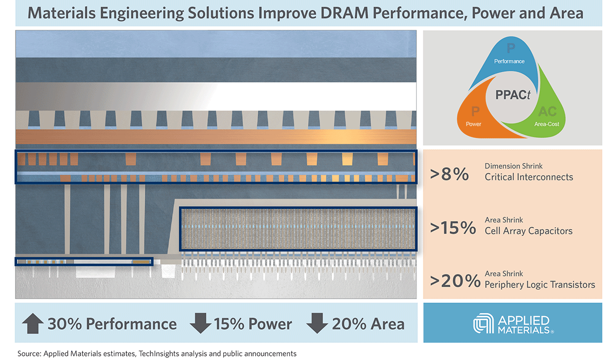
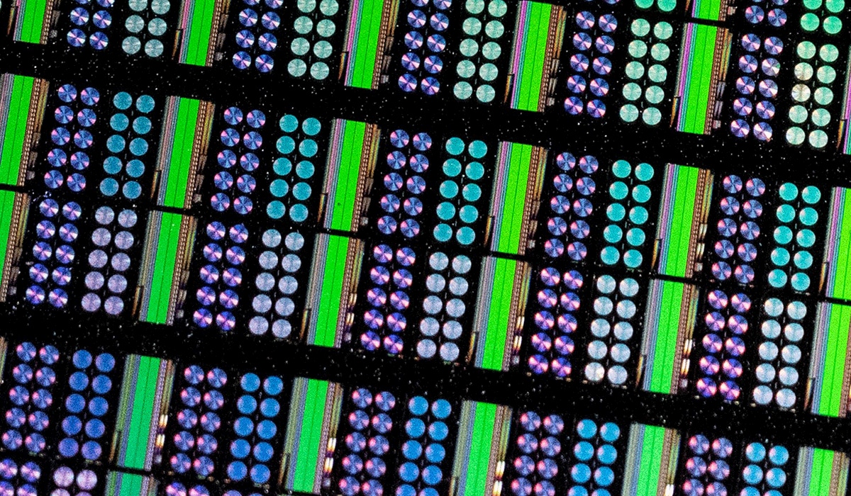
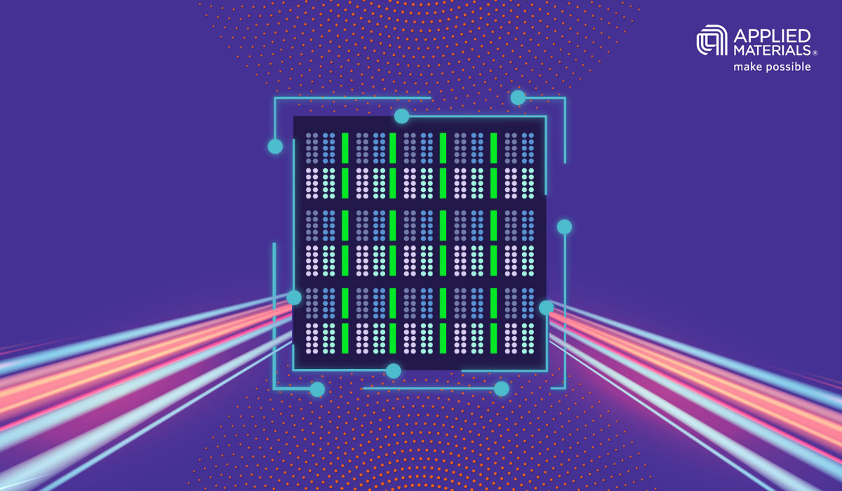
Introducing Breakthroughs in Materials Engineering for DRAM Scaling
To help the industry meet global demand for more affordable, high-performance memory, Applied Materials today introduced solutions that support three levers of DRAM scaling.