Products & Technologies
Products & Services
Contact
Products & Services
Products & Technologies
Services
Resources
Contact
Posted
April 03, 2019

Stay updated on our content.
Manufacturing Requirements of New Memories

by Gill Lee
Apr 03, 2019
After decades of research and development, three new types of memory—magnetic RAM (MRAM), phase change memory (PCRAM) and resistive RAM (ReRAM)—are moving toward commercial adoption, making this an exciting time for the semiconductor and computing industries. All three of these emerging memories are enabled by new materials and will require breakthroughs in process technology and manufacturing.
The ideal semiconductor memory would offer all of the following characteristics:
- Fast read speed
- Fast write speed
- Random access
- Low cost
- 3D scalability
- Low power
- Non-volatility
- High endurance
- High temperature tolerance
- Multiple states (for storing multiple bits)
In reality, no memory offers all of these attributes, and this applies to existing and emerging memories alike. Chip and computer designers will continue to use a variety of memory technologies to achieve their goals. Let’s examine the characteristics of the three emerging memories to anticipate where they are likely to find applications in the industry.
MRAM: A Leading Candidate for IoT Devices
MRAM has a number of attractive attributes: it is fast (random reads and writes); non-volatile and low power (magnetic technology); and offers low cost potential since the memory array can be embedded in the back-end interconnect layer of the chip with only three additional masks.
Compared to SRAM, it is slower, but fast enough to be a working memory for many embedded computing applications, and is also potentially fast enough for Level 3 cache needs.
In fact, several leading logic/foundry companies have announced early production of system-on-chip designs that use embedded MRAM. Specifically, MRAM is becoming a leading candidate for Internet of Things (IoT) devices which will increasingly need to support artificial intelligence (AI) computation. Over time, MRAM may prove capable of meeting the high temperature requirements of the automotive segment of the embedded market.
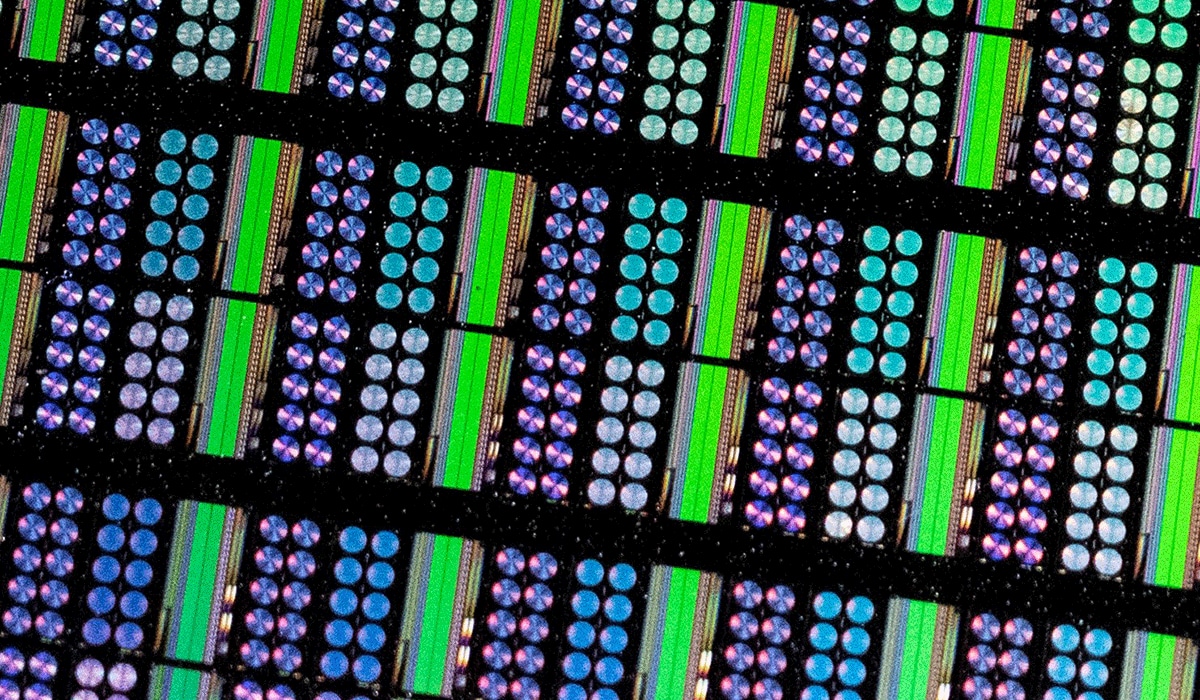
From a technology and manufacturing perspective, the biggest challenge of MRAM is precisely depositing the many film stacks needed to form the magnetic tunnel junction (MTJ) which is the basic programming element used to represent digital data. Many metal and insulating layers need to be deposited using physical vapor deposition (PVD) methods in pristine, sub-atmospheric, high vacuum conditions. Each layer must be precisely controlled and measured. Most importantly, the core magnesium oxide (MgO) film layer needs to be deposited in a precise and nearly crystalline arrangement with stringent control since even a single atom of height variation can greatly affect performance and reliability.
PCRAM: A New Storage Class Memory
PCRAM is based on “phase change” materials that transition from highly amorphous material arrangements to crystalline arrangements with heat as the programming mechanism.
PCRAM offers the attributes of random access, low cost compared to DRAM, 3D scalability and non-volatility. As a result, leading memory companies are evaluating PCRAM’s suitability for applications such as non-volatile DIMM to replace part of the DRAM-based DIMM and high-end solid state drives.
PCRAM requires multiple layers of material to be precisely deposited to create critical structures. While the PCRAM layers are not as thin as MRAM, the materials are highly susceptible to impurities, and this calls for a PVD process technology capable of working with multiple materials and preventing particles and impurities. Once the PCRAM stack has been formed, plasma etching is used to form the individual memory cells, and encapsulation protects the exposed phase change materials.
Scalability is key to driving the PCRAM cost roadmap. 2D scaling has been used to reduce critical dimensions to 20nm half-pitch, with 15-16nm design rules on the horizon. 3D scaling of PCRAM is even more promising: initial designs have used 2-layer stacks, but technology roadmaps suggest that stacks of 4 or even 8 layers are possible.
ReRAM Targets High Density Applications
ReRAM technology comes in several forms. Some ReRAMs are embedded in a metal filament within an ionic bridge. Others are formed as oxygen vacancies produced within a base material. Bits are stored in the resistive materials, often metal oxide; programming is done by applying electric current to the resistive materials; and reading is done by sensing different levels of resistance. One other aspect of ReRAM is that a broad range of materials can be used for this technology.
To date, ReRAM has exhibited endurance limitations and work is still needed to identify the failure mechanisms so that materials and manufacturing technology can be refined to ensure reliability in the field. Assuming these challenges are solved, ReRAM promises to bring high density and low cost to storage applications.
Today’s mainstream memories—DRAM, Flash and SRAM—took decades to mature and continue to evolve. They are becoming more difficult to scale, however, notably in terms of performance, power and cost. At the same time, computing continues to expand, and many envision a world where tens of billions of low-cost computers are embedded into all kinds of industrial and consumer products, creating the IoT and fueling an explosion of data that needs to be stored in public and private cloud data centers. Emerging memories like MRAM, PCRAM and ReRAM are leading candidates to complement and, in some cases, replace today’s mainstream technologies—promising higher performance, lower power and lower cost.
Emerging memory technologies will take advantage of new materials and structures that will be formed using precise film deposition, measurement, etch/removal and encapsulation—in pristine conditions. In fabricating these next-generation memories, variations of even a few atoms make a very big difference. Applied Materials is committed to enabling our customers with new materials engineering solutions, and my colleagues and I plan to share more with you in the weeks and months ahead.
Tags: MRAM, PCRAM, ReRAM, memory
Gill Lee
Managing Director, Technical Marketing / Strategic Programs - Semiconductor Products Group

Gill Lee is managing director of technical marketing / strategic programs in the Semiconductor Products Group at Applied Materials. He joined Applied in 2009, having worked previously in memory technology development at Qimonda/Infineon/Siemens in New York, France and Germany. Gill earned his M.S. in materials science and engineering from POSTECH University, South Korea. He has authored a number of papers on CMOS integration and process development and holds several related patents.
Now is the Time for Flat Optics
For many centuries, optical technologies have utilized the same principles and components to bend and manipulate light. Now, another strategy to control light—metasurface optics or flat optics—is moving out of academic labs and heading toward commercial viability.
Seeing a Bright Future for Flat Optics
We are at the beginning of a new technological era for the field of optics. To accelerate the commercialization of Flat Optics, a larger collaborative effort is needed to scale the technology and deliver its full benefits to a wide range of applications.
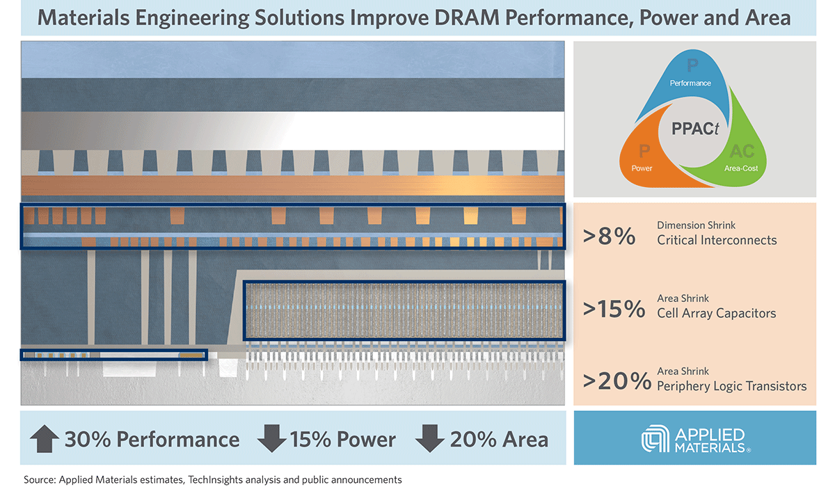
Introducing Breakthroughs in Materials Engineering for DRAM Scaling
To help the industry meet global demand for more affordable, high-performance memory, Applied Materials today introduced solutions that support three levers of DRAM scaling.