Products & Technologies
Products & Services
Contact
Products & Services
Products & Technologies
Services
Resources
Contact
Posted
January 23, 2019

Stay updated on our content.
Technology Trends and Innovations in 2019

Jan 23, 2019
Big Data and Artificial Intelligence (AI) are fueling a new computing revolution, which is transforming many industries from transportation to healthcare. In 2019, the pace of this change will accelerate, creating new challenges and also tremendous opportunities for innovation.
Virtually all electronic devices are becoming smarter and more connected. This is causing an explosion of machine-generated data that now exceeds data generated from humans. The challenge is how to capture, store and process the very large data sets at virtually real-time speed. This will take a lot of storage, along with new types of memory and order of magnitude improvements in computing performance per watt.
But just as momentum is building to drive the AI revolution, classic Moore’s Law scaling is slowing. While 2D shrinking previously delivered the required improvements in PPAC (performance, power and area/cost) for the PC era, the industry now needs new methods of driving chip improvements beyond Moore’s Law. This will involve a combination of approaches: new chip architectures, 3D design techniques, novel materials, new ways to continue shrinking transistors, and advanced packaging schemes to connect chips together in new ways. We call this the “New Playbook” for semiconductor design and manufacturing. Enabling this new playbook will require major advances in materials engineering and greater collaboration across the industry ecosystem.
One of the biggest challenges for the semiconductor industry is how to enable faster processing speeds without raising the power envelope. Today there’s a 1,000X gap in compute performance per watt that must be closed. Lowering power consumption will involve design changes at the chip- and system-level and innovations in materials and structures within the device. This is one of the critical hurdles that must be solved to unlock the potential of AI and Big Data.
New materials and architectures being developed focus on delivering PPAC solutions for the industry. For example, replacing copper with cobalt as a new material in the lower level wiring layers of a device reduces resistance and improves the RC delay problem, which results in higher speed and lower power consumption. A move to horizontal gate-all-around devices reduces transistor leakage providing further improvements in power and performance. Packaging is another key enabling area which provides systems solutions that bring logic and memory together for higher performance and lower power while also addressing form-factor requirements. Stacking DRAM chips together has brought about High Bandwidth Memory (HBM) which combined with logic in interposer designs has delivered major performance gains for AI computing.
With regard to materials, the days of working with individual materials from the periodic table are over. Continued advances in PPAC require new combinations of materials that work together to form novel structures with precise electrical properties. Assembling these new material combinations to achieve predictable properties and interactions is an increasingly complex task requiring Integrated Materials Solutions that can co-optimize multiple process steps, often within the same platform and under vacuum. More and more, engineering materials in vacuum permits precise engineering at the atomic-level.
Applied is expanding its capabilities to help enable the new semiconductor industry playbook. To collaborate with more customers on projects that can speed availability of new materials and process technologies, Applied announced plans for the new Materials Engineering Technology Accelerator (META Center) in November of last year. The META Center will complement and extend the capabilities of Applied’s Maydan Technology Center in Silicon Valley. Applied is also enabling advanced packaging capabilities with a full suite of 300mm advanced wafer level packaging equipment and personnel in Singapore. Our venture capital arm, Applied Ventures, is investing in AI chip startups with disruptive innovations in computing architecture. Last year Applied launched the AI Design Forum at SEMICON West to bring together design and manufacturing experts—from materials to systems—under one umbrella to collaborate at a higher level.
2019 is a pivotal year for semiconductors, where major collaborative efforts and innovations in manufacturing technologies will impact a wide range of industries. By providing breakthroughs in materials engineering, Applied is at the forefront of enabling the technologies shaping the future.
Tags: AI, artificial intelligence, Big Data, Moore's Law, META Center, Integrated Materials Solutions
Sundeep Bajikar
Corporate Vice President, Corporate Strategy and Marketing

Sundeep is Head of Corporate Strategy and Marketing (CSM) and guides the executive leadership team in the development of the company's growth thesis, strategic priorities, key initiatives and investor communications. He is also responsible for developing Applied’s marketing capabilities and community. Sundeep’s work served as the foundation for Applied’s strategies related to AI, ICAPS, Heterogenous Integration and Net Zero.
He joined Applied in 2017 after spending ten years as a Senior Equity Research Analyst covering global technology stocks, including Apple and Samsung Electronics, for Morgan Stanley and Jefferies. Previously he worked for a decade as a researcher, ASIC design engineer, system architect and strategic planning manager at Intel Corporation.
Sundeep holds an MBA in finance from The Wharton School and M.S. degrees in electrical engineering and mechanical engineering from the University of Minnesota. He holds 13 U.S. and international patents with more than 30 additional patents pending. Sundeep is also author of a book titled, “Equity Research for the Technology Investor – Value Investing in Technology Stocks.” He was an Institutional Investor Rising Star.
Now is the Time for Flat Optics
For many centuries, optical technologies have utilized the same principles and components to bend and manipulate light. Now, another strategy to control light—metasurface optics or flat optics—is moving out of academic labs and heading toward commercial viability.
Seeing a Bright Future for Flat Optics
We are at the beginning of a new technological era for the field of optics. To accelerate the commercialization of Flat Optics, a larger collaborative effort is needed to scale the technology and deliver its full benefits to a wide range of applications.
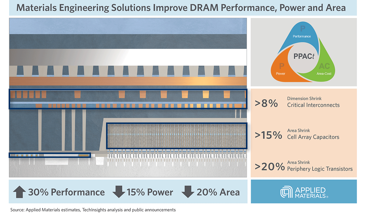
Introducing Breakthroughs in Materials Engineering for DRAM Scaling
To help the industry meet global demand for more affordable, high-performance memory, Applied Materials today introduced solutions that support three levers of DRAM scaling.