Products & Technologies
Products & Services
Contact
Products & Services
Products & Technologies
Services
Resources
Contact
Posted
January 31, 2020

Stay updated on our content.
Delivering the Next Billion-Unit Computing Platform Requires Industry Collaboration

by Kevin Moraes
Jan 31, 2020
Happy New Year!
The last IEDM of the past decade has given us a technology roadmap to industry growth opportunities and technology challenges in the new decade ahead.
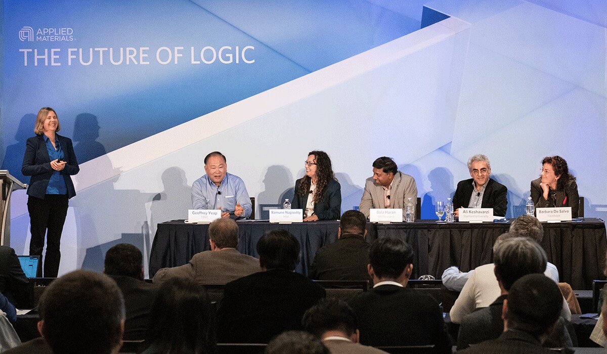
Moderated by my colleague, Regina Freed, the panel was titled, “The Future of Logic: EUV is Here, Now What?” Regina was joined by experts from Facebook, IBM Research, Intel, Stanford University and TSMC. The points of view shared during the lively discussion showed that while there is no single path to achieving continued improvements in chip performance, power and area-cost (PPAC), the industry will be well-served to search for solutions together.
The call to action is already evident at the dawn of 2020, as the Internet of Things (IoT), Big Data and AI have the potential to transform every area of the economy and our lives in ways far greater than previous generations of computing. The 1980s and 1990s gave us the PC era, client-server computing and the Internet, with annual unit sales in the hundreds of millions. That was followed in the 2000s and 2010s by the smartphone, social media and cloud computing, where yearly unit sales surpassed one billion.
The new decade will usher in the most significant transformation yet as capabilities like augmented reality, edge computing and AI create hundreds of billions of smart devices and new applications that will fundamentally change human-to-human communication and machine-to-machine communication—all wirelessly and at the edge of the network.
With each computing era comes new demands on logic technology and the surrounding memory and storage architectures. For PCs it was the shift to high-gigahertz processors and bigger hard disk drives. Smartphones put a premium on battery life and form factor, with Arm chips, the foundry model and NAND flash enabling what has become a 1.5 billion unit per year platform. Supporting this evolution was improvements in semiconductor technology through 2D scaling and new materials and structures in the transistor, interconnect and memory.
Now, the transition to the AI Era is once again challenging industry conventions governing semiconductor design and manufacturing.
This brings us back to the overarching question Applied Materials posed to the panelists at IEDM: “EUV is here, now what?” Geoffrey Yeap, Senior Director of Advanced Technology at TSMC, said that while EUV helps in some areas, such as lowering mask count, it exposes a host of other issues that need to be solved. “Ultimately, we need a better transistor that is more energy efficient and higher performance. And interconnect resistance remains very, very high. If we don't solve the interconnect problem, we won't have a better transistor.”
Echoing this sentiment was Ramune Nagisetty, Senior Principal Engineer and Director of Process and Product Integration Technology Development Group at Intel, who said, “Parasitic resistance and capacitance issues that come from device scaling will not be handled with EUV.”
“Apart from performance, I think there are two other things which EUV is not going to solve,” added Bala Haran, Master Inventor and Director of Silicon Process Research at IBM Research. “One is reliability. Especially for high-performance compute, reliability is extremely important. And that's a materials challenge. The other is routability. Design routability improves with EUV, but it's not completely solved.”
Barbara De Salvo, Silicon Technology Strategist, Augmented-Reality-Virtual-Reality Silicon Division at Facebook, outlined the technical requirements of what she believes could be the next billion-unit platform: augmented-reality glasses. Barbara observed that smart glasses have distinct system and software needs that must be addressed to enable features such as gesture recognition and a new class of biometric-based applications, including haptics, enhanced perception, contextual awareness and even virtual whiteboard projection.
“I don't think that what we are seeing today in the market is satisfying the need to achieve this goal, at least in terms of performance or power. The power requirement alone is really well beyond what exists today,” she said. “And we need a lot of computing power with very little latency, because we have to actually reconstruct reality.”
This raised an interesting “chicken-and-egg” problem: how can the industry fund the next round of silicon innovations when fabs are increasingly expensive to build and operate, and are still supported by the high-volume economics of the smartphone?
Speaking to the evolution of the smartphone, Ramune said, “That form factor is the one that is really driving the leading-edge node development at the foundries. There's a bit of a circular thing here where there needs to be a big customer with big pull if you really want a specialized technology node that's targeted for your application.”
“AR/VR and edge devices have long standby times, which means leakage is extremely important,” said Barbara of Facebook. “This is something that has not been so far addressed, because most of Moore's Law is really done for high performance. I think that if we want to address a new market we need, in some way, to customize the core technology.”
TSMC enables high-volume platforms, according to Geoffrey. “We will fully customize for an application based on a common platform where you have the largest common denominator for yield and for process reuse to reduce cost. Even right now at 5nm, we will serve mobile and 5G but also the data center, AI and high-performance computing. The platform is still similar.”
“I think a path forward is to develop the capabilities that enable edge intelligence, such that we take computing locally to the endpoint device,” said Ali Keshavarzi, Adjunct Professor in the Electrical Engineering Department of Stanford University. “The benefit of doing this is we can have more devices that can create growth in the semiconductor industry.”
In order to address the PPAC requirements of a diverse set of applications, Applied Materials believes the industry needs a new playbook for semiconductor design and manufacturing. This new playbook involves a combination of approaches including new system architectures, new 3D structures, new materials, new ways to shrink transistors and new ways to connect chips together with advanced packaging.
Accelerating the new playbook will require greater collaboration across the technology ecosystem—from materials to systems. To that end, Applied Materials recently opened the Materials Engineering Technology Accelerator (META Center), a state-of-the-art facility where we are working across a diversity of companies and engineering disciplines to speed the development and prototyping of new chip materials, architectures and devices. This is especially important to help address the “chicken-and-egg problem” for emerging applications with distinctly different PPAC requirements that need access to a facility where new technologies can be piloted for transfer to high-volume customer fabs.
“Even at the level of R&D, I strongly recommend having a whole system approach,” Facebook’s Barbara said. “This question is interesting because there are new actors coming into the semiconductor market, like Facebook. And I think that the future ecosystem will be different than what we had in the past.”
We at Applied Materials couldn’t agree more.
Stay tuned for the next blog in this series where we will take a deep dive into another key topic discussed by the panel: design challenges of the IoT and edge AI products.
Tags: IEDM, logic, Facebook, TSMC, PPAC, IBM, Research, Intel, Stanford University, AI, Big Data, new materials, augmented reality, New Playbook, Moore’s Law, iot, EUV, META Center
Kevin Moraes
Corporate Vice President, Strategy and Marketing, Semiconductor Products Group

Dr. Kevin Moraes serves as Corporate Vice President of Strategy and Marketing at Applied Materials, leading global initiatives that drive growth across key semiconductor segments. In this role, he aligns market insights with business priorities, shapes competitive positioning, and enables customer success through technology inflections. Previously, he held leadership positions in product management and technology development within the company. He earned a Ph.D. in materials science and engineering from Rensselaer Polytechnic Institute, an MBA from the University of California, Berkeley, and a bachelor’s degree in chemical engineering from Annamalai University.
Now is the Time for Flat Optics
For many centuries, optical technologies have utilized the same principles and components to bend and manipulate light. Now, another strategy to control light—metasurface optics or flat optics—is moving out of academic labs and heading toward commercial viability.
Seeing a Bright Future for Flat Optics
We are at the beginning of a new technological era for the field of optics. To accelerate the commercialization of Flat Optics, a larger collaborative effort is needed to scale the technology and deliver its full benefits to a wide range of applications.
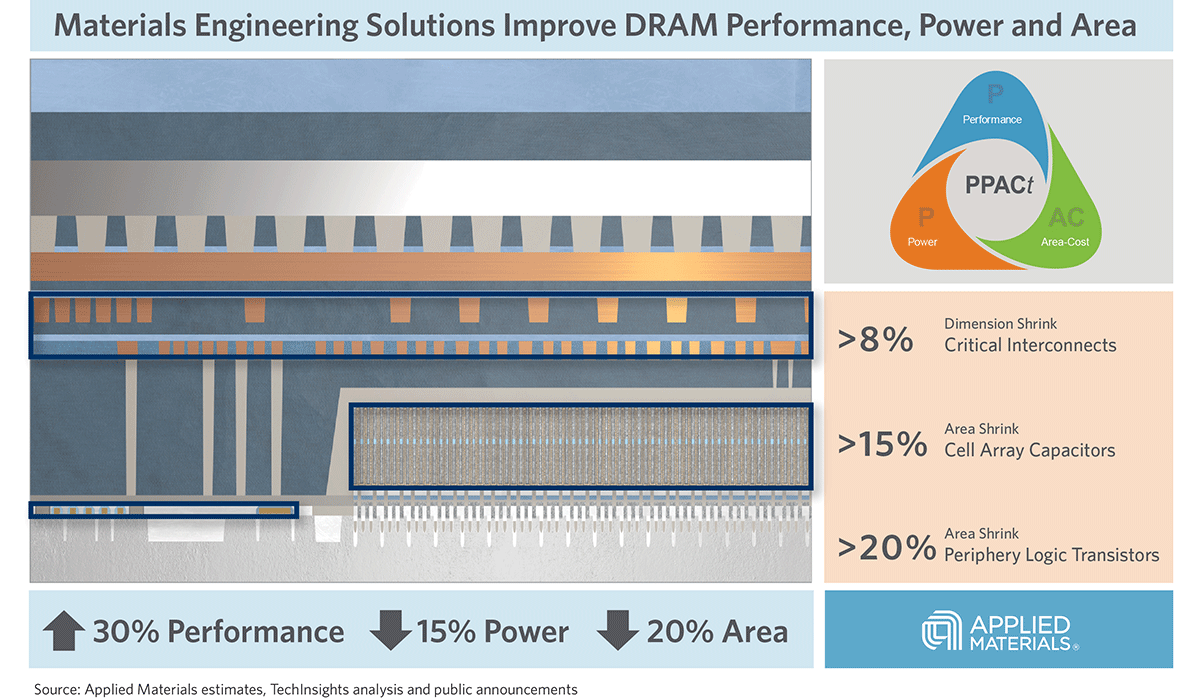
Introducing Breakthroughs in Materials Engineering for DRAM Scaling
To help the industry meet global demand for more affordable, high-performance memory, Applied Materials today introduced solutions that support three levers of DRAM scaling.