半導體 (Semiconductor)
解決方案與軟體
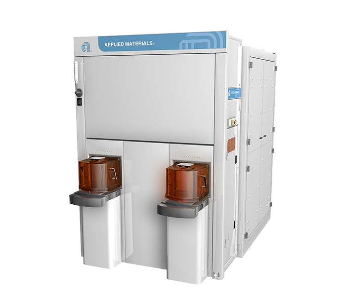
SEMVision H20 缺陷分析
在當今最先進的節點中,光學檢測在區分缺陷與製程變異雜訊時能力有限,因此會產生高誤報率或高滋擾率的密集缺陷圖。因此,交付電子束審查的缺陷候選數量從十倍增至百倍。製程控制工程師越來越需要能夠在保持大量生產所需速度和靈敏度的同時,可分析急遽加樣本的缺陷檢測系統。
SemVision H20 缺陷複檢系統採用冷場發射 (CFE) 電子束技術,實現次奈米解析度以辨識最微小的深層缺陷。SemVision H20引入第二代 CFE 技術,在保持高靈敏度和次奈米解析度的同時,提供更快的成像速度。憑藉更快的晶圓採樣能力,晶片製造商可以在更短的時間內收集相同的資訊量。
為了補充先進的成像功能,SemVision H20 整合了深度學習 AI 功能,能夠自動從誤報缺的缺陷中擷取出真實缺陷,從而實現更準確、有效率的缺陷表徵。晶片製造商可以使用自己的缺陷影像或設計模擬來訓練 AI 模型,提供系統學習的靈活度,並提高分選準確度。
H20 加入了 SEMVision 系列,這是全球最先進、應用最廣的電子束複檢系統。G7 將繼續為成熟的技術節點提供服務,而採用CFE 技術的 SemVision H20 則開創了複雜 3D 架構變革的新時代,包括新型環繞式閘極 (GAA) 電晶體,以及行程更高密度的 DRAM 和 3D NAND 記憶體。
- 1 / 4
- 2 / 4
- 3 / 4
- 4 / 4