半導體 (Semiconductor)
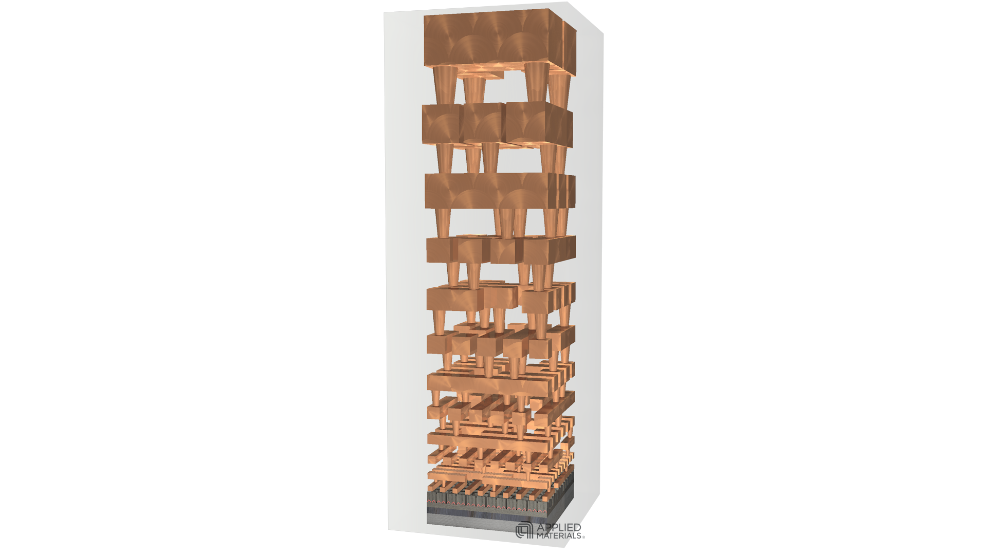
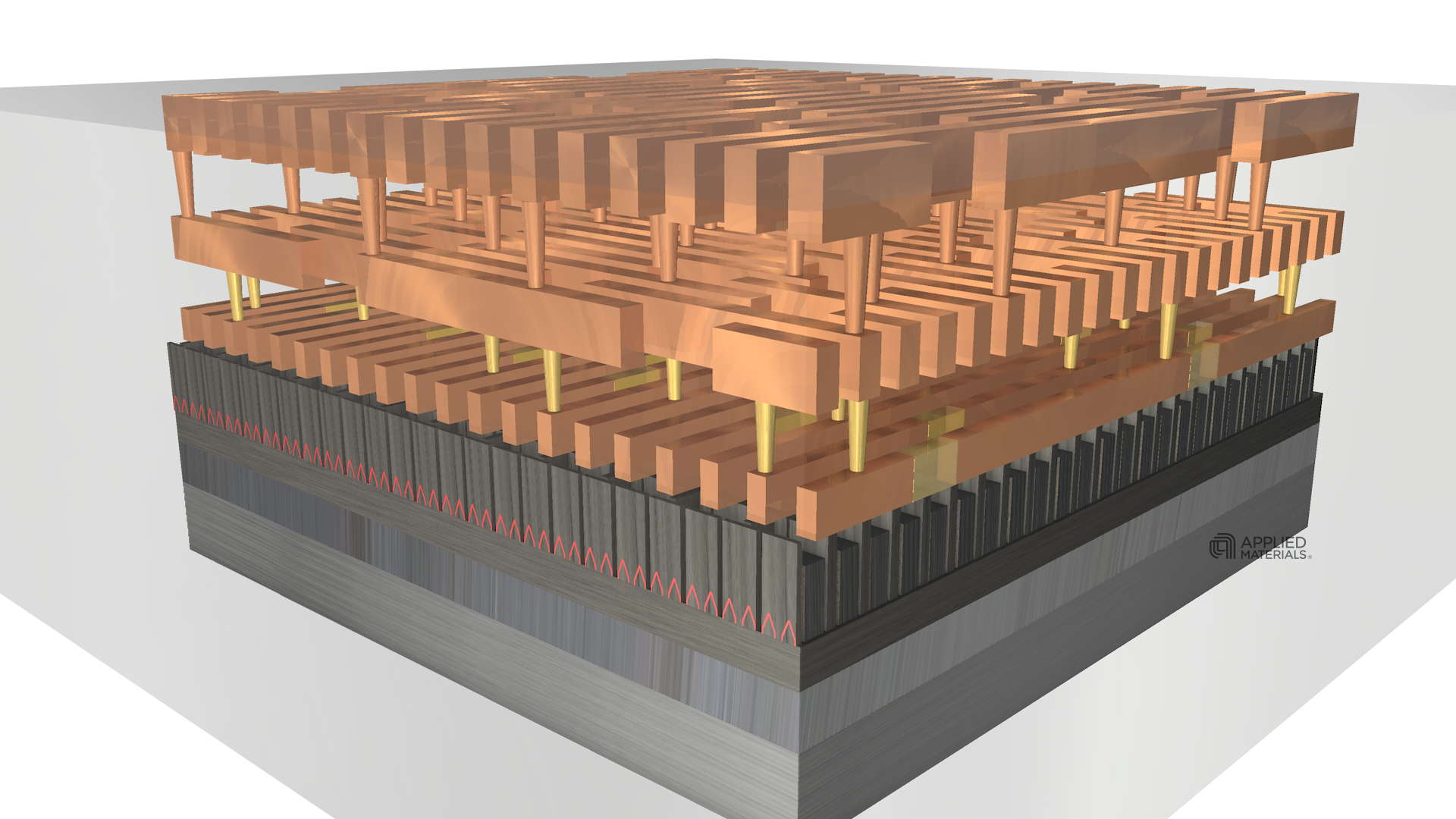
Patterning Technologies and Device Scaling
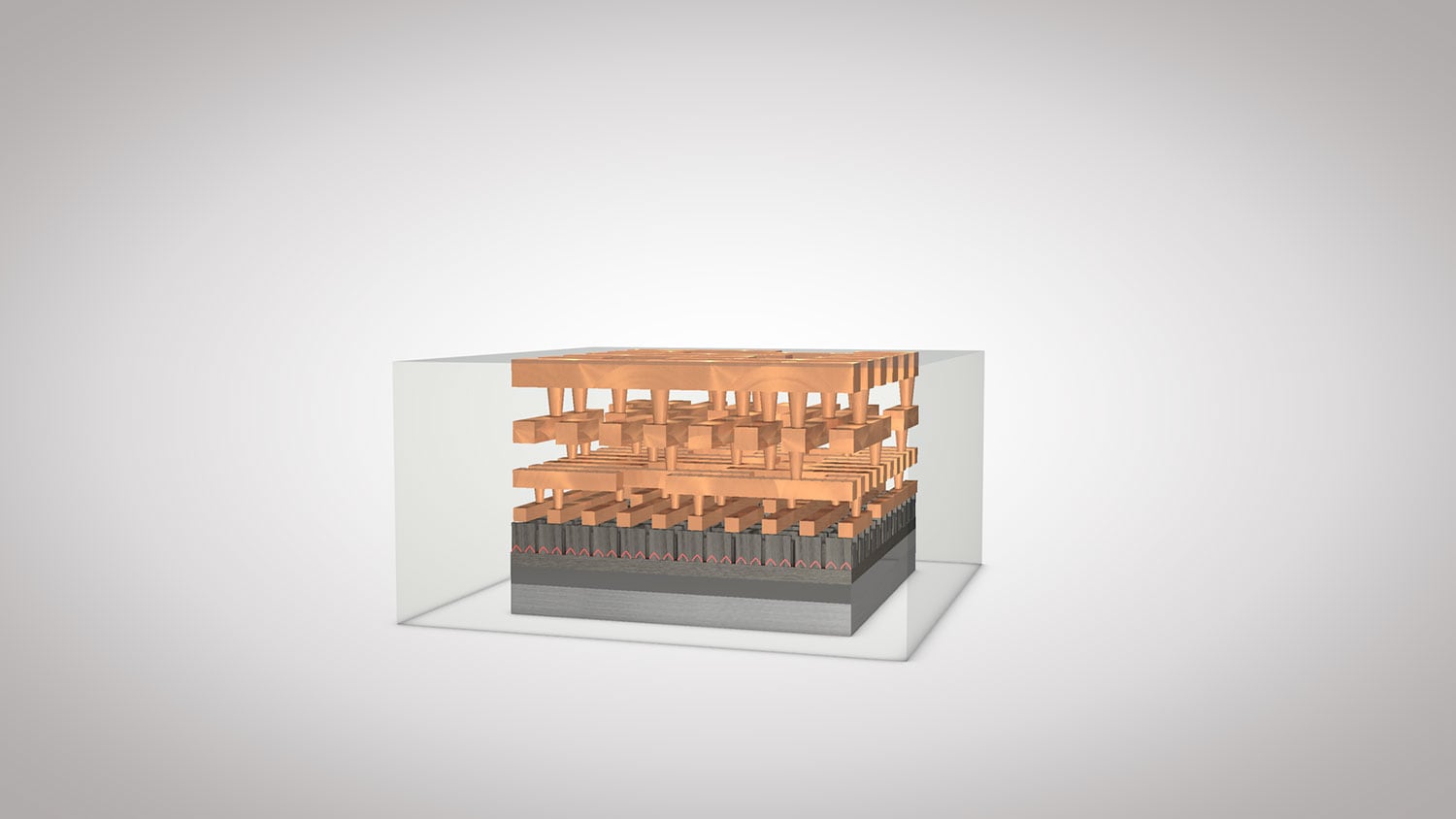
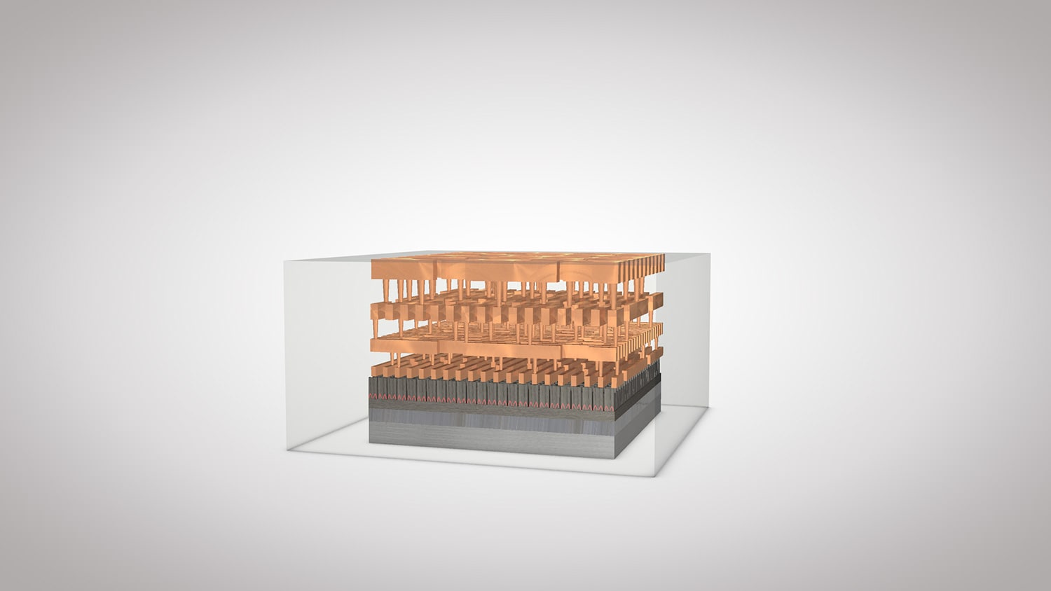
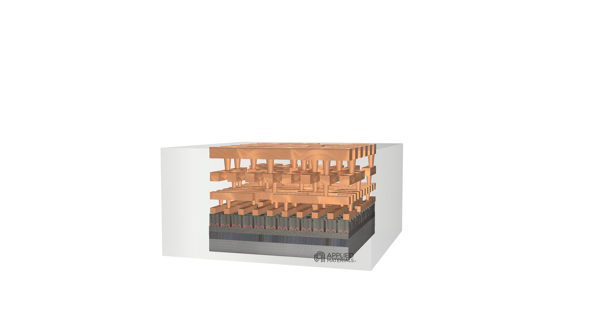
As we progress from 14 to 7nm devices and beyond, SADP and SAQP will be required for some layers and LE with either 193i or EUV lithography for others.
EUV will likely be used to create cuts and vias in some of the lower metal layers.
14nm Video 1280 x 720
7nm Video 1280 x 720
