
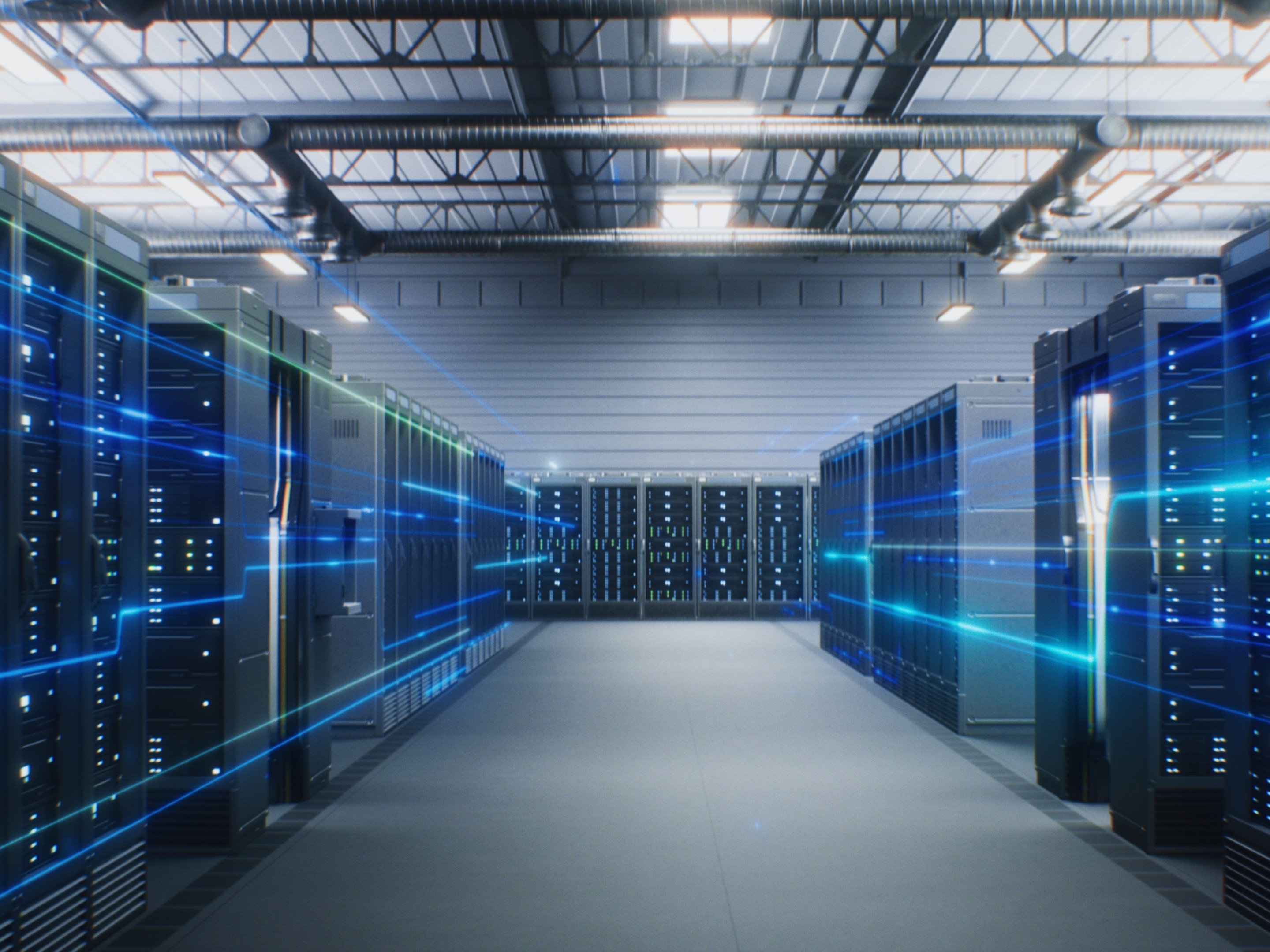
오늘날의 AI 데이터센터는 엄청난 양의 데이터를 처리하고, 이동 및 저장해야 합니다. 이 모든 것은 반도체 기술 혁신 덕분에 가능합니다.
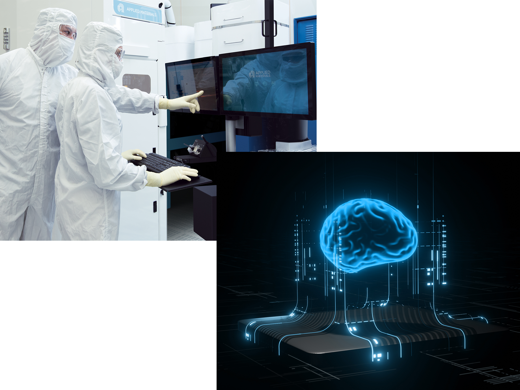
AI는 반도체 로드맵을 재편하고 칩 설계 및 제조 방식을 바꾸고 있습니다.
어플라이드의 전략은 이러한 변곡점에 초점을 맞춘 혁신입니다. 기초 반도체 기술은 반도체 성능 향상, 컴퓨팅 속도 증가, 데이터센터 및 엣지 컴퓨팅 환경에서의 AI 비용 절감에 매우 중요한 역할을 합니다.
우리는 어플라이드 리더십의 다섯 가지 핵심 영역이 AI 시스템의 아키텍처를 정의할 것이라 믿습니다.


AI는 모든 산업과 기업, 그리고 개인의 일상에 필수적인 요소이며, 어플라이드 머티어리얼즈는 AI 시대의 기반입니다. 모든 AI 혁신 뒤에는 반도체 혁신이 있고, 반도체 혁신 뒤에는 어플라이드의 재료 공학 혁신이 있습니다. 우리는 재료 혁신을 통해 세상에 실질적이고 의미 있는 변화를 만들어냅니다.


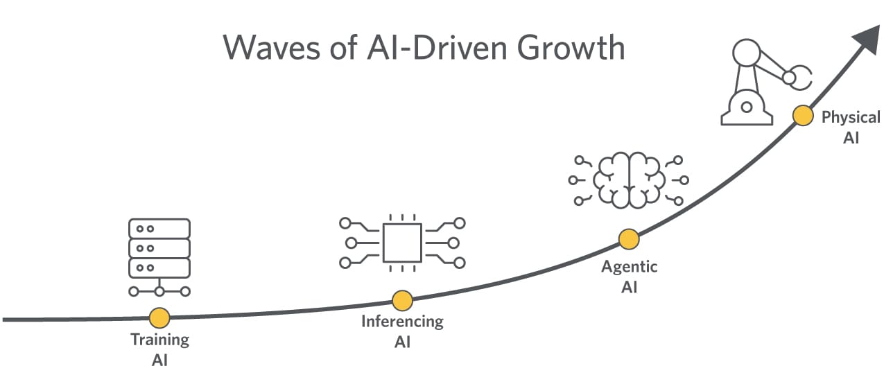
AI는 우리가 살아가는 시대에 가장 큰 기술적 변곡점입니다. AI는 산업 구조를 바꾸고 세계 경제를 재편하게 될 것입니다. AI는 응용 분야와 산업을 넘어 그 기반이 되는 컴퓨팅 자체에도 영향력을 미치고 있습니다. 반도체 칩은 성능 향상 뿐 아니라 에너지 효율성의 획기적인 개선을 통해 컴퓨팅 기능을 향상시켜야 합니다.
AI 워크로드가 증가하고 있는 가운데, 오늘날 에이전틱, 에지, 피지컬 AI와 같은 새로운 애플리케이션이 향후 수년간 산업 성장을 견인할 것입니다. AI 데이터센터는 2030년까지 전 세계 전력 공급량의 10% 이상을 소비할 수 있습니다.
어플라이드 머티어리얼즈는 칩 제조사가 원자 단위로 재료를 형상화하고 변형할 수 있도록 지원하는 혁신적이고 광범위한 장비 솔루션 포트폴리오를 제공합니다. 이를 통해 에너지 효율적인 컴퓨팅에 대한 요구를 해결하고 있습니다. 오늘날의 AI 데이터센터는 더 많은 트랜지스터, 더 빠른 인터커넥트, 그리고 향상된 전력 효율성을 요구하는 만큼 정밀성이 더욱 중요해지고 있습니다.
이러한 변화에는 새로운 재료, 구조 및 통합 방식이 필요합니다. 재료 과학과 혁신은 생태계 전반에 걸쳐 기존 기술 체계를 변화시키고 재편하는 핵심 동력입니다. 새로운 반도체 칩과 패키징 기술의 효율성이 향상되면서 AI 성능도 함께 발전하고 있습니다.
첨단 AI 칩을 위한 새로운 반도체 아키텍처 이면에서는 다양한 재료 기술이 동시에 변곡점을 맞이했으며, 이는 전례 없는 복잡성과 그에 따른 정밀도를 필요로 합니다. 이것은 그 어느 때보다 더 많은 재료 공학 혁신이 필요하다는 것을 의미합니다.
나노미터 단위의 공간에 여러 재료를 배치하려면 극도의 정밀도가 요구되는데, 이는 재료의 특성과 상호작용 방식이 모든 것을 좌우하기 때문입니다. 트랜지스터에서 웨이퍼, 그리고 팹에 이르기까지 혁신이 가속화됨에 따라, 원자 수준의 제어를 유지하면서도 놀라운 속도로 발전이 이루어지고 있습니다. 이 새로운 세상에서는 모든 옹스트롬이 차이를 만듭니다.

- 1 / 5
- 2 / 5
- 3 / 5
- 4 / 5
- 5 / 5


AI는 우리가 살아가는 시대에 가장 큰 기술적 변곡점입니다. 어플라이드 머티어리얼즈의 역할은 심도 있는 재료 과학 전문성과 철저한 운영 역량을 바탕으로 기술 변곡점 기반의 혁신을 주도하는 것입니다. 이를 통해 오늘날 급증하는 AI 처리 수요를 뒷받침하는 성능과 에너지 효율성, 신뢰를 제공합니다.
혁신을 위한 새로운 R&D 모델
실리콘밸리에 위치한 어플라이드의 EPIC 센터는 미국 내 역대 최대 규모의 첨단 반도체 장비 R&D 투자 사례입니다. AI 시대의 속도에 맞춰 설계된 EPIC은 재료공학 혁신이 상용화되기까지의 기간을 수십 년에서 수년으로 줄입니다.
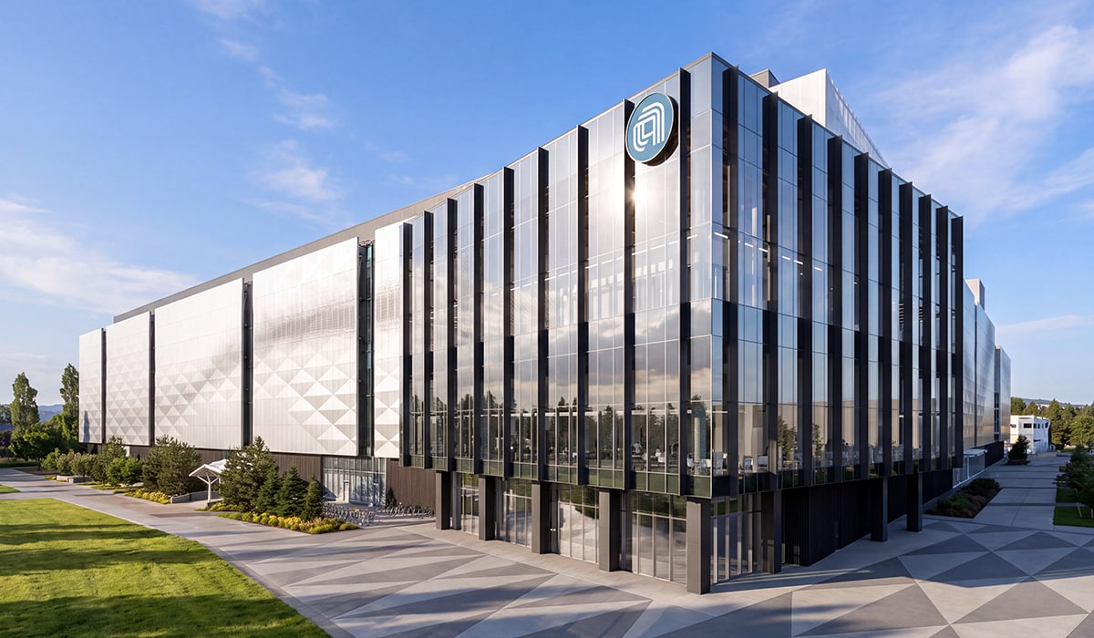
어플라이드 머티어리얼즈 EPIC 센터
어플라이드는 R&D의 공식을 새로 쓰고 고객 및 파트너와 함께 혁신하는 방식을 바꿈으로써, 아이디어에서 칩 상용화에 이르는 가장 빠른 길을 만들어가고 있습니다. 새로운 EPIC 센터 자세히 알아보기