Products & Technologies

Products & Services
Company
Contact
Products & Services
Products & Technologies
Services
Resources
Company
Contact
Today's AI Data Centers Must Process, Move And Store Massive Amounts Of Data. All Of This Enabled By Semiconductor Technology Innovation.

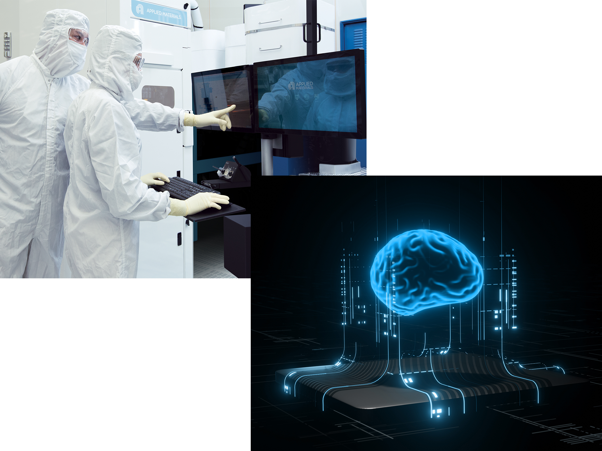
AI Is Reshaping The Semiconductor Roadmap And Changing The Way Chips Are Designed And Manufactured.
Applied's strategy is inflection-focused innovation. Foundational semiconductor technology plays a critical role in increasing semiconductor performance, increasing speed of compute and bringing down the cost of AI in the data center and at the edge.
There Are Five Key Areas Of Applied Leadership That We Believe Will Define The Architecture Of AI Systems:


AI is fundamental to every industry, every company, and every person and Applied Materials is the foundation of the AI era. Behind every AI breakthrough is a semiconductor breakthrough, and behind those breakthroughs are materials engineering innovations from Applied. It is through our material innovation that we make a real, meaningful difference to the world.


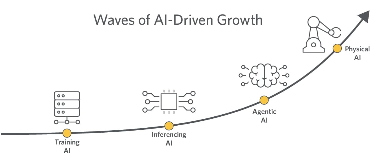
AI is the most profound technology inflection of our lifetime. It will change industries and redefine the global economy. The impact of AI extends beyond applications and industries to the underlying computing itself. Semiconductor chips must deliver improvements in computing capability, not just through performance, but also through dramatically improved energy efficiency.
AI workloads are growing and today we see new, incremental applications like agentic, edge and physical AI growing the industry over the next several years. AI data centers could consume more than 10% of global electricity supply by 2030.
Applied Materials is solving this need for energy-efficient computing by delivering our innovative, broad portfolio of equipment solutions that enables chipmakers to shape and modify materials atom by atom. In today’s AI data centers, this precision matters when more transistors, faster interconnects and increased power efficiency are expected.
This transformation demands new materials, architectures and integration approaches. Materials science and innovation are the primary drivers disrupting and reshaping the traditional technology stack across the ecosystem. Advances in AI performance are enabled by new semiconductor chip and packaging technology efficiencies.
Think about this: beneath every new semiconductor architecture for advanced AI chips, multiple materials inflections are happening in parallel, creating unprecedented complexity and requiring unprecedented precision. That's more materials engineeringr innovation than ever before.
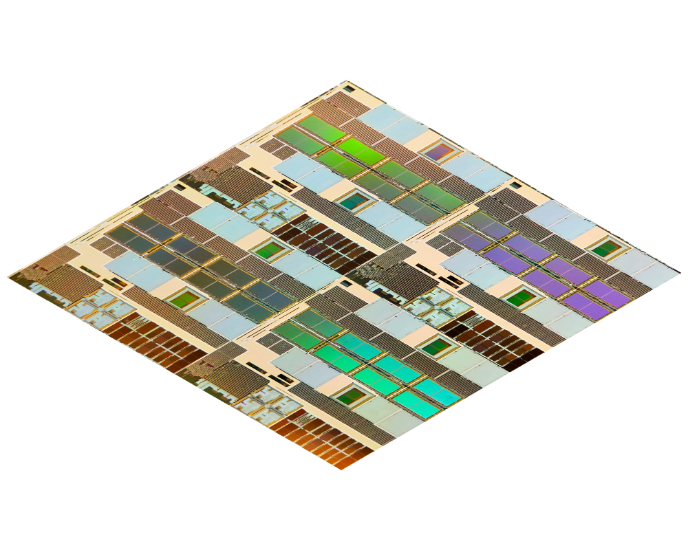
Placing multiple materials within a space of the size of a nanometer requires extraordinary accuracy, because material properties—and how they interact—make all the difference. As innovation accelerates from transistors to wafers to fabs, progress is occurring at a mind-bending pace while maintaining atomic-level control. In this new world, every angstrom matters.


- 1 / 5
- 2 / 5
- 3 / 5
- 4 / 5
- 5 / 5


AI is the largest technology inflection of our lifetime. The role of Applied Materials is to drive inflection-based innovation through our deep materials science expertise and the operational discipline to deliver the performance, energy-efficiency, and reliability needed to meet today's advanced AI workloads.
A New R&D Model for Innovation
Applied’s EPIC Center in Silicon Valley represents the largest-ever U.S. investment in advanced semiconductor equipment R&D. Built for the demands of the AI era, so the next breakthrough in materials science reaches the world in years rather than decades.

Applied Materials EPIC Center
By reinventing R&D and changing the way we innovate with our customers and partners, we are creating the fastest path from concept to commercialized chip. Read more about the new EPIC Center.