Products & Technologies

Products & Services
Company
Contact
Products & Services
Products & Technologies
Services
Resources
Company
Contact
Intensely Focused on Innovation
As a global technology leader, research and development is the lifeblood of our company. Applied Materials has a proven track record of innovation and industry breakthroughs that have significantly contributed to the growth of the semiconductor industry. At Applied, we deliver material innovation that changes the world.
With our deep expertise in materials engineering, and the broadest portfolio of capabilities, Applied is constantly developing solutions that solve our customers’ high-value problems. Staying close to our customers, understanding their toughest challenges and working to develop innovative products are keys to our success.
In labs around the world, Applied’s scientists are developing technologies and using materials in ways no one would have thought possible. Our patent portfolio is the strongest in our industry, demonstrating the creativity and dedication of our engineering community to push the boundaries of what’s possible to achieve the next technology breakthrough. We build an innovation network through venture investments and joint research and development programs with customers, partners, universities and research institutes.
>23,500
PATENTS


Transforming the World with Semiconductors
Applied’s focus on advancing semiconductor technology is transforming nearly every aspect of our lives. Semiconductors are the “brains” of modern electronics enabling advances in communications, computing, healthcare, transportation, clean energy, and countless other applications.
Our R&D capabilities help achieve innovative breakthroughs. For instance, in 1984, mobile phones weighed about 2.5 pounds, sold for $4,000 and held a charge for only about 30 minutes of talk time. Compared to your smartphone today, the difference is tremendous. In fact, a single smartphone today has far more computing power than the computers used by NASA to land a person on the moon in 1969. Smarter, faster and more energy-efficient chips are enabling life-changing innovations.
Global R&D Locations
We’ve created advanced R&D facilities around the world to enhance our collaboration with chipmakers and ecosystem partners to help move inventions from idea to market faster.

Maydan Technology Center
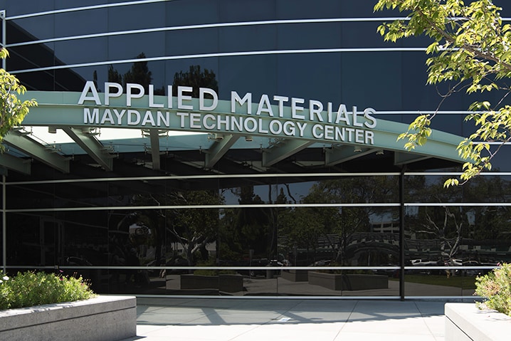
Maydan Technology Center
For over 20 years, the Maydan Technology Center (MTC) has been a state-of-the-art facility designed to accelerate our customers’ time to market. It is the heart of Applied’s innovation engine, where more than 500 Applied engineers collaborate alongside our customers to bring new semiconductor process technology to life.
On the cutting edge of rapid testing and development, MTC is both a fab and a test lab, which allows customers to test each manufacturing step under one roof. With more than 120 chip manufacturing tools and over 80 metrology instruments, the Center provides customers with a unique capability to speed transitions to new technologies, shorten cycle times to production and bring new products to market with reduced risk.
META Center
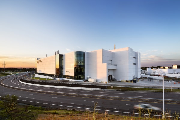
Materials Engineering Technology Accelerator (META Center)
The Materials Engineering Technology Accelerator is a world-class hub for innovation in materials engineering R&D. The META Center accelerates the availability of new chipmaking materials and process technologies that empower breakthroughs in semiconductor performance, power and cost.
The Center focuses on solutions development for both traditional semiconductor device inflections as well as other industrial initiatives, such as ICAPS (IoT, communications, automotive, power and sensors) and artificial intelligence (AI) spaces.
This first-of-its-kind facility, located in Albany, New York, features a broad suite of Applied’s most advanced process systems along with complementary technologies needed for new chip materials and structures.
Advanced Packaging Development Center
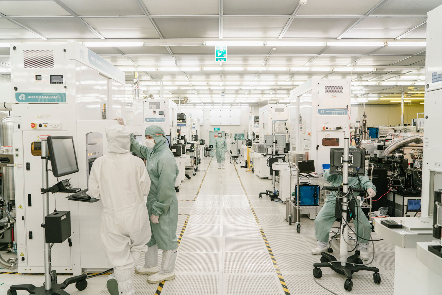
Advanced Packaging Development Center
The Advanced Packaging Development Center is a state-of-the-art cleanroom that is among the most advanced wafer-level packaging labs in the world. It houses the industry’s broadest portfolio of products that enable the foundational building blocks of heterogeneous integration, including advanced bump and micro-bump, fine-line redistribution layer (RDL), TSV and hybrid bonding.
As computing has progressed from PCs to mobile devices and now to AI, we’re seeing the rise of heterogeneous design, which has designers rethinking how to best integrate both chips and systems. Heterogeneous design and advanced packaging are now a competitive imperative for the world’s leading semiconductor and systems companies and the Advanced Packaging Development Center gives Applied a unique ability to optimize and validate process technologies.
The Center was established as a joint lab partnership with the Institute of Microelectronics (IME), a research institute of Singapore’s Agency for Science, Technology and Research (A*STAR).
Tainan Display Manufacturing Center and Lab
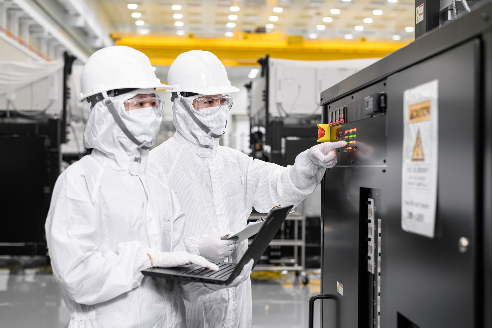
Tainan Display Manufacturing Center and Lab
Displays provide a window between people and the information universe. Humans crave information and we live in an era where digital information - entertainment, news, education, social networking, and much more–is readily available. Tainan Display Lab (TDL) plays a strategic role in employing deep display expertise to enable the next generation of displays. It is the world’s first combined display equipment manufacturing facility and R&D laboratory.
TDL plays a key role in advancing improvements such as image resolution and quality, size increases, and new form factors as the display industry has evolved from CRTs to LCDs, and now to OLED. These innovations, along with reduced costs, have enabled new products and driven the proliferation of displays that create dynamic and stunning visual experiences for consumers.
The facility, which includes two cleanrooms and a laboratory is located close to customers in the Tainan Science Park, to provide fast support to our display customers throughout Asia.
EPIC
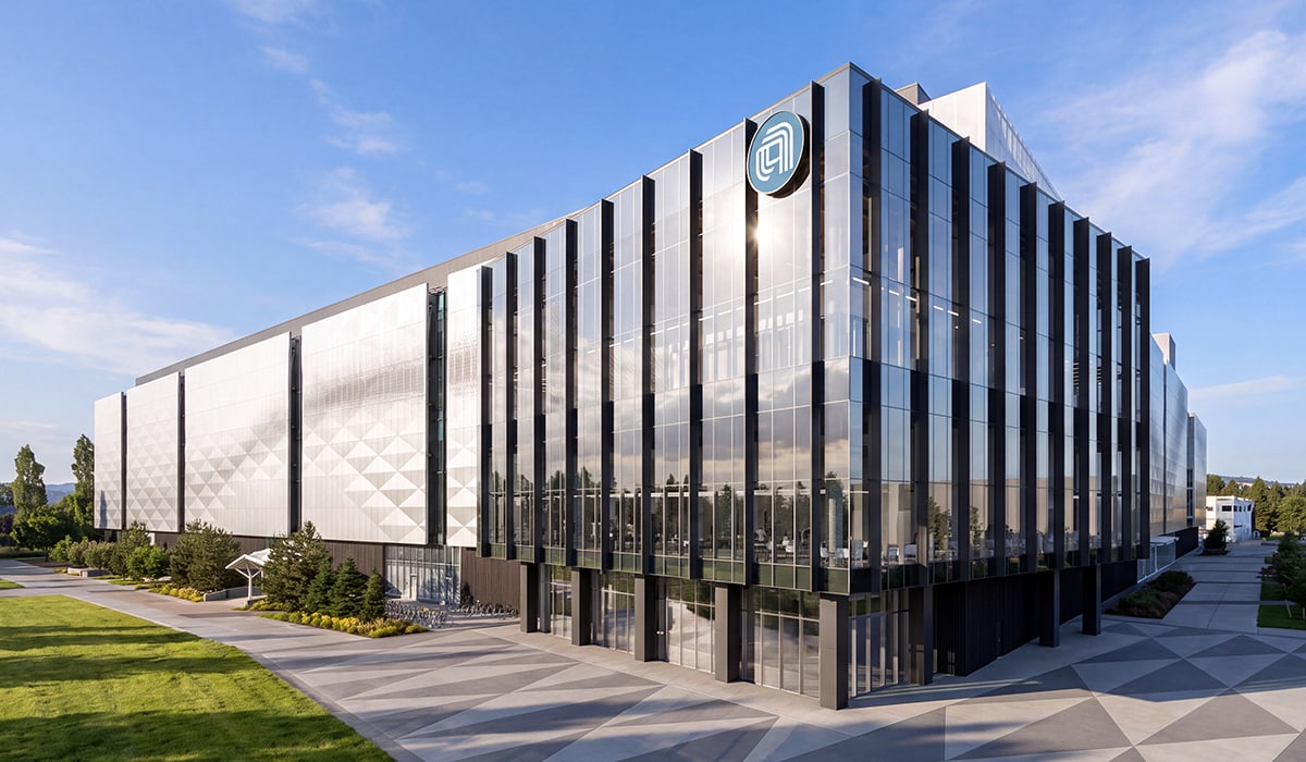
The Equipment and Process Innovation and Commercialization (EPIC) Center is one of the world’s largest facilities dedicated to secure, collaborative semiconductor process technology and manufacturing equipment R&D. Inside the EPIC Center, the world’s leading chipmakers, systems companies, equipment partners and university researchers work side by side with Applied’s scientists and engineers to accelerate the pace of chip innovation for the AI era.
EPIC is designed to reinvent the R&D model the semiconductor industry has relied on for decades. In the traditional model, foundational research happens in one environment, equipment and process development in another, and integration and pilot production in a third, with a careful handoff at every phase. The EPIC Center is designed to remove these handoffs, putting the people who invent the materials, build the equipment, and make the chips together in a state-of-the-art facility purpose-built for commercialization.
-
Maydan Technology Center
-
META Center
-
Advanced Packaging Development Center
-
Tainan Display Manufacturing Center and Lab
-
EPIC
Maydan Technology Center
For over 20 years, the Maydan Technology Center (MTC) has been a state-of-the-art facility designed to accelerate our customers’ time to market. It is the heart of Applied’s innovation engine, where more than 500 Applied engineers collaborate alongside our customers to bring new semiconductor process technology to life.
On the cutting edge of rapid testing and development, MTC is both a fab and a test lab, which allows customers to test each manufacturing step under one roof. With more than 120 chip manufacturing tools and over 80 metrology instruments, the Center provides customers with a unique capability to speed transitions to new technologies, shorten cycle times to production and bring new products to market with reduced risk.
Materials Engineering Technology Accelerator (META Center)
The Materials Engineering Technology Accelerator is a world-class hub for innovation in materials engineering R&D. The META Center accelerates the availability of new chipmaking materials and process technologies that empower breakthroughs in semiconductor performance, power and cost.
The Center focuses on solutions development for both traditional semiconductor device inflections as well as other industrial initiatives, such as ICAPS (IoT, communications, automotive, power and sensors) and artificial intelligence (AI) spaces.
This first-of-its-kind facility, located in Albany, New York, features a broad suite of Applied’s most advanced process systems along with complementary technologies needed for new chip materials and structures.
Advanced Packaging Development Center
The Advanced Packaging Development Center is a state-of-the-art cleanroom that is among the most advanced wafer-level packaging labs in the world. It houses the industry’s broadest portfolio of products that enable the foundational building blocks of heterogeneous integration, including advanced bump and micro-bump, fine-line redistribution layer (RDL), TSV and hybrid bonding.
As computing has progressed from PCs to mobile devices and now to AI, we’re seeing the rise of heterogeneous design, which has designers rethinking how to best integrate both chips and systems. Heterogeneous design and advanced packaging are now a competitive imperative for the world’s leading semiconductor and systems companies and the Advanced Packaging Development Center gives Applied a unique ability to optimize and validate process technologies.
The Center was established as a joint lab partnership with the Institute of Microelectronics (IME), a research institute of Singapore’s Agency for Science, Technology and Research (A*STAR).
Tainan Display Manufacturing Center and Lab
Displays provide a window between people and the information universe. Humans crave information and we live in an era where digital information - entertainment, news, education, social networking, and much more–is readily available. Tainan Display Lab (TDL) plays a strategic role in employing deep display expertise to enable the next generation of displays. It is the world’s first combined display equipment manufacturing facility and R&D laboratory.
TDL plays a key role in advancing improvements such as image resolution and quality, size increases, and new form factors as the display industry has evolved from CRTs to LCDs, and now to OLED. These innovations, along with reduced costs, have enabled new products and driven the proliferation of displays that create dynamic and stunning visual experiences for consumers.
The facility, which includes two cleanrooms and a laboratory is located close to customers in the Tainan Science Park, to provide fast support to our display customers throughout Asia.
The Equipment and Process Innovation and Commercialization (EPIC) Center is one of the world’s largest facilities dedicated to secure, collaborative semiconductor process technology and manufacturing equipment R&D. Inside the EPIC Center, the world’s leading chipmakers, systems companies, equipment partners and university researchers work side by side with Applied’s scientists and engineers to accelerate the pace of chip innovation for the AI era.
EPIC is designed to reinvent the R&D model the semiconductor industry has relied on for decades. In the traditional model, foundational research happens in one environment, equipment and process development in another, and integration and pilot production in a third, with a careful handoff at every phase. The EPIC Center is designed to remove these handoffs, putting the people who invent the materials, build the equipment, and make the chips together in a state-of-the-art facility purpose-built for commercialization.