Products & Technologies
Products & Services
Contact
Products & Services
Products & Technologies
Services
Resources
Contact
Selective Deposition
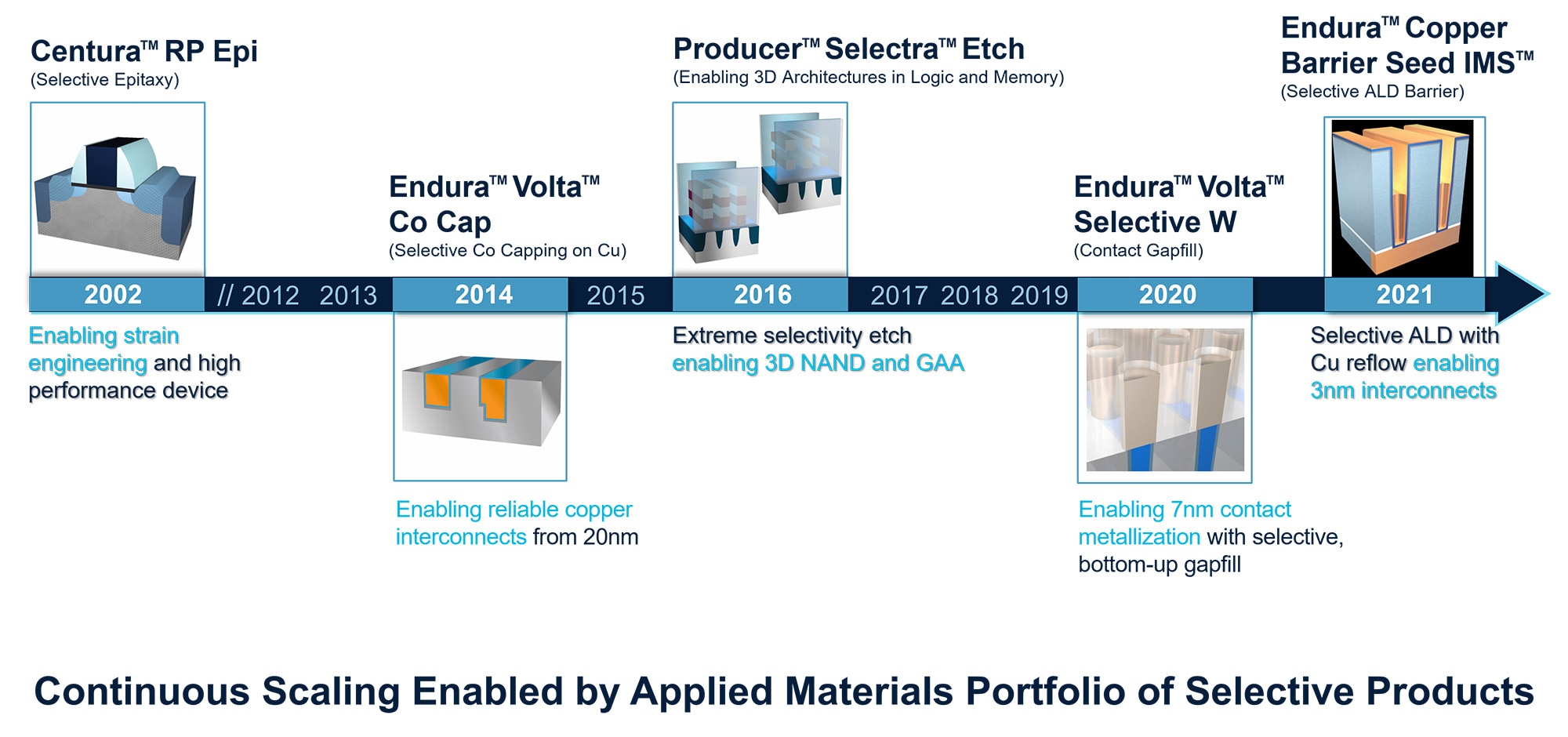
Complex patterning schemes, higher aspect ratios, smaller vias and channels, more fragile features, and the increasing risk of pattern collapse are hastening the transition from bulk materials engineering to selective processing.
Selective processes use co-designed chemical and materials interactions to enable delicate and precise deposition and removal of target materials. Selective deposition and epitaxy is additive manufacturing at an atomic scale, putting atoms only where they are needed. Selective etch is subtractive manufacturing at an atomic scale, removing only unwanted atoms—even those beyond the line of sight—and leaving the rest in place. Selective deposition, epitaxy and etch technologies can be used to create and shape tiny patterns; fabricate novel structures; and overcome technology roadblocks such as the pattern collapse associated with wet processes, edge-placement errors in patterning, and 2D scaling issues associated with transistor contact and interconnect resistance.
Applied leads the industry in selective deposition and selective epitaxy processes. The Endura Copper Barrier Seed IMS™ replaces standard high-resistance via interfaces with a low-resistance selective ALD barrier to enable interconnect metallization for 3nm and beyond. Similarly, the Endura Volta Selective W CVD system replaces conventional metal and dielectric liners and barriers with selective Tungsten deposition to lower contact resistivity and reduce the bottleneck of 2D scaling. The Endura Volta CVD Cobalt system provides a robust seed layer for copper lines and selective Cobalt cap to strengthen adhesion at the copper-dielectric interface. Finally, the Centura Prime Epi system plays a critical role in strain engineering Si-Ge channel performance found in FinFET and GAA transistors.