Products & Technologies
Products & Services
Contact
Products & Services
Products & Technologies
Services
Resources
Contact
Producer® Onyx®

- 1 / 4
- 2 / 4
- 3 / 4
- 4 / 4
- Innovative film treatment improves chip wiring insulation to enable longer battery life for mobile devices
- Advances low k technology for scaling logic chips to 22nm node and beyond
- Increases mechanical strength of chip for higher packaging yield
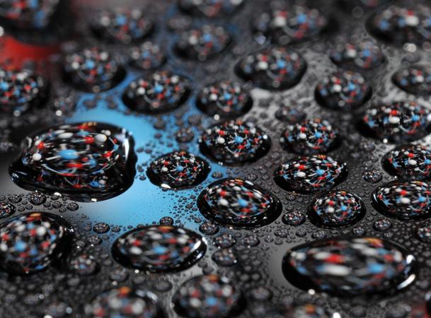
In integrated circuits, current-carrying copper wiring is insulated by dielectric (non-conducting) materials. As semiconductor devices scale down, the ability to increase device speed is significantly affected by the dielectric constant (k) of the dielectric, which must scale down correspondingly. Chip makers have progressively reduced the insulating film’s k value from 4.0 for silicon dioxide materials to 3.5 by adding fluorine at 180nm, to 3.0 by incorporating carbon at 90/65nm, to 2.5 by introducing porosity at 45/32nm. Porous low-k dielectrics are now the foundation for building copper interconnects. For the 2x nm technology node, ultra-low-k materials (k~2.2) will be needed to achieve the requisite capacitance reduction.
These low-k materials are exposed to more than 150 process steps in fabricating a 10-12 metal-layer structure, and must then withstand the stresses of packaging and assembly. Plasma etch, photoresist ash, wet clean, chemical mechanical planarization, and copper oxide removal prior to barrier deposition can disrupt the chemical structure of surface layers of the low-k film.
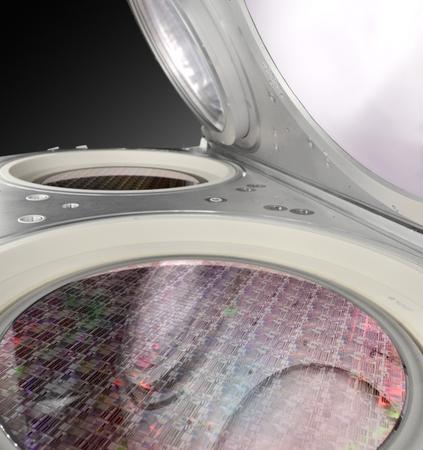
Applied Producer Onyx is a novel process for treating the low-k film to restore its chemical integrity and enhance its robustness. The Onyx process treats not only the surface of the film but also the bulk film, thus enabling the lowest integrated k, while enhancing key structural properties like modulus and hardness.
With this treatment, Producer Onyx ensures that the resultant low-k dielectric meets 2x nm requirements for local interconnect formation as well as the subsequent advanced packaging steps. Furthermore, it enhances the productivity of other processes (e.g., etch) by counteracting effects that would otherwise decrease yield.
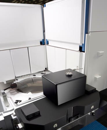
The Onyx process is performed using the production-proven, high-throughput Producer GT platform. With its innovative Twin Chamber® architecture, this platform enables simultaneous processing of up to six wafers for superior productivity.