Products & Technologies
Products & Services
Company
Contact
Products & Services
Products & Technologies
Services
Resources
Company
Contact
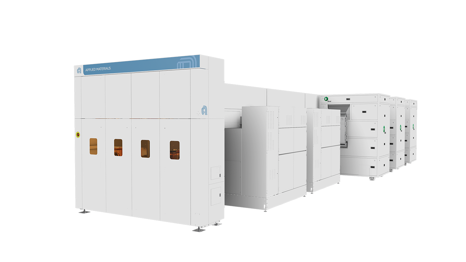
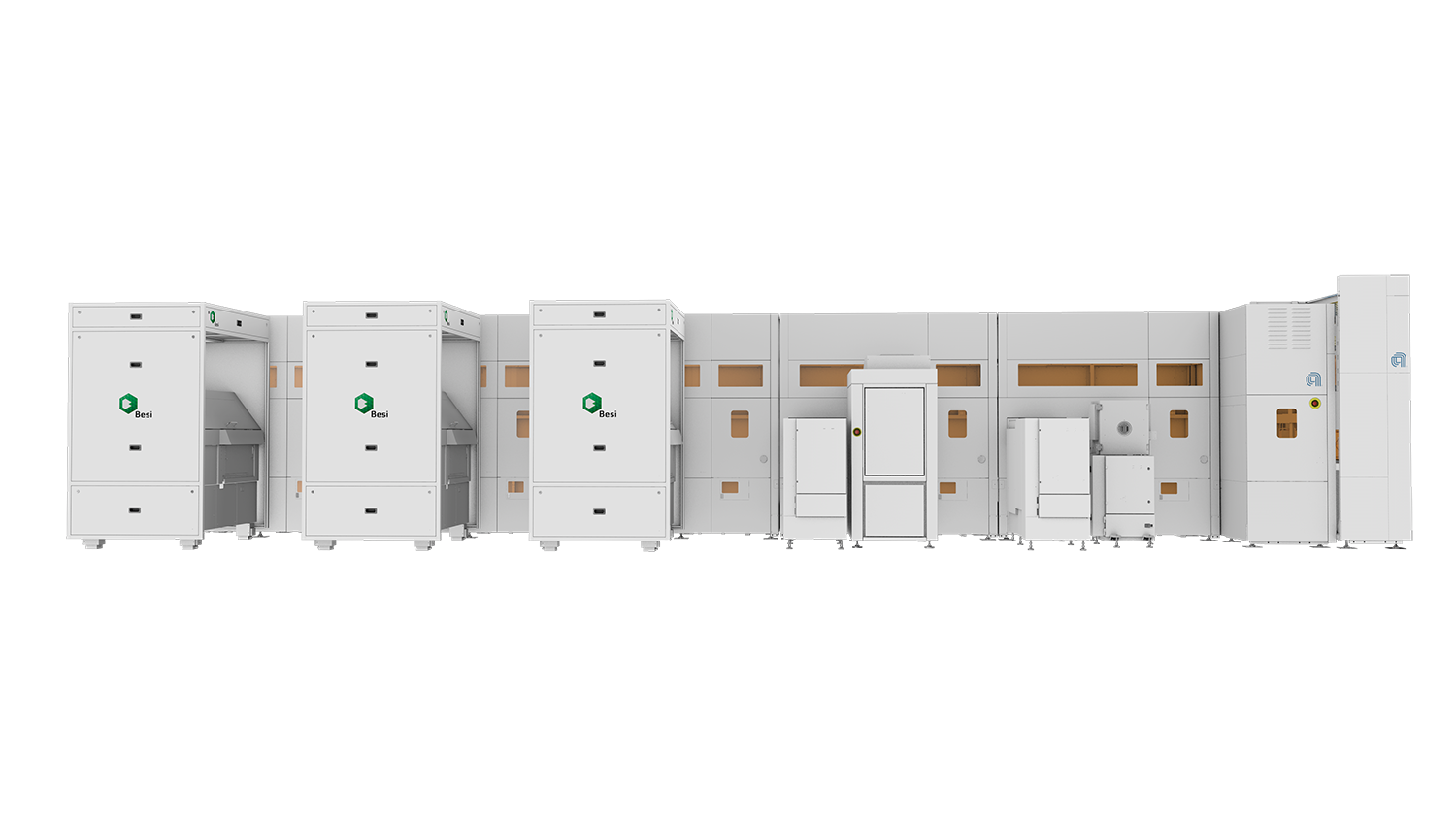
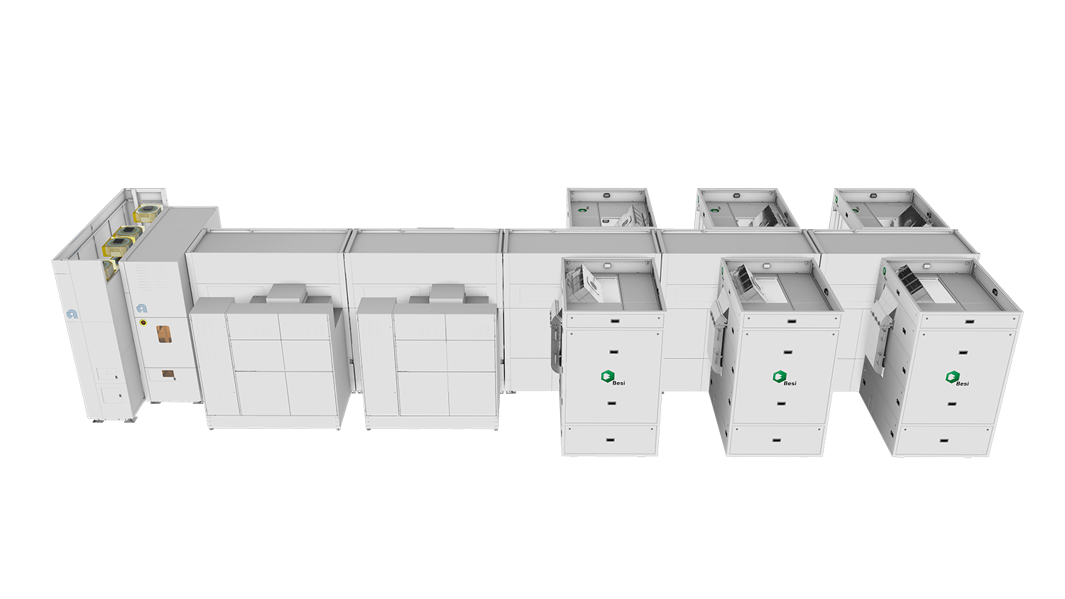
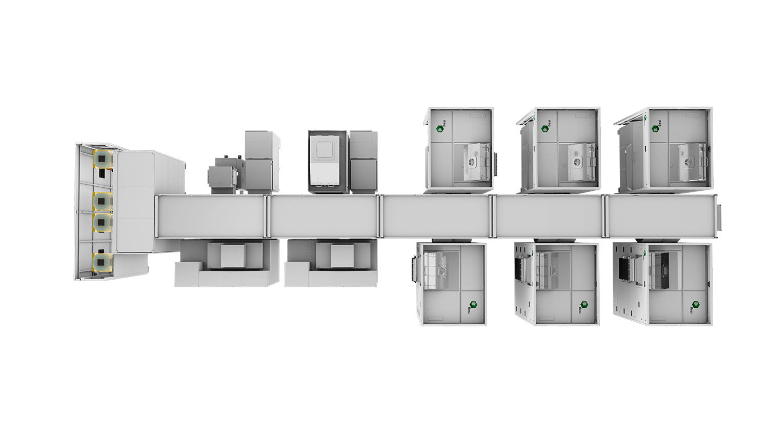
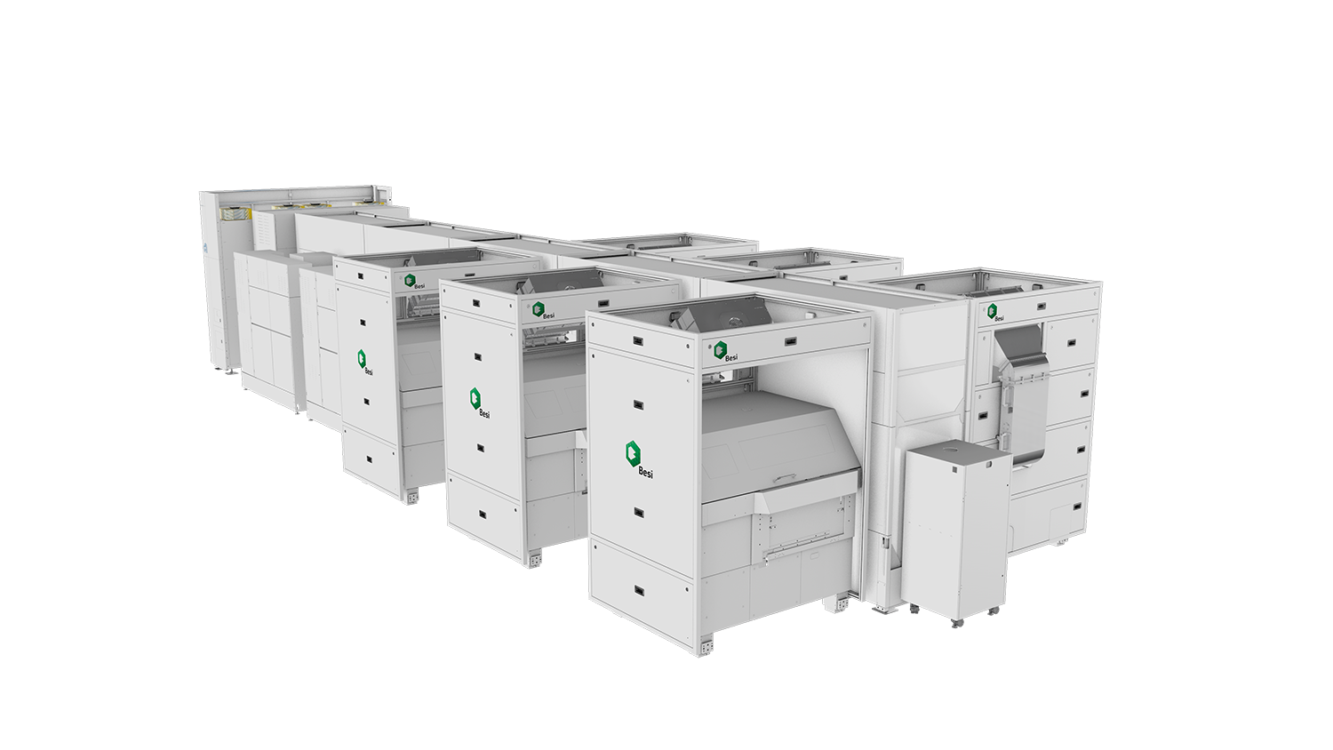
Kinex Integrated Die-to-Wafer Hybrid Bonding System
Semiconductor packaging is evolving to support increasingly complex, heterogeneous architectures. Driven by high-performance computing (HPC), AI accelerators, and stacked memory such as high-bandwidth memory (HBM), new bonding solutions are needed to support yield, accuracy and scalability. The rise of chiplet-based designs and multi-die packages introduces challenges in queue time management, die-level traceability, and bonding precision. Customers require a high-volume manufacturing (HVM) solution that can address these demands while maintaining cleanliness and minimizing defects. Kinex™ was developed to meet these challenges head-on, enabling next-generation hybrid bonding for advanced logic, memory, and emerging applications like photonics and microdisplays.
Kinex is Applied Materials’ fully integrated hybrid bonding system, purpose-built for HVM environments. Co-developed with BE Semiconductor Industries N.V. (Besi), the industry leader in hybrid bonding, Kinex combines best-in-class bonding accuracy, advanced queue-time control, and exceptional system cleanliness. Its modular architecture supports many chiplets per module and integrates wet clean, plasma activation, and in-situ metrology for real-time overlay control. Kinex’s smart sequencer and AIx-powered software suite enable predictive maintenance, die-level traceability, and multi-binning capabilities.
Kinex is optimized for a wide range of applications including 3D integrated circuits, HBM, co-packaged optics (CPO), and sensor integration. Its flexible configuration supports both single-layer and multi-layer bonding flows, with validated performance on silicon, III-V materials, and glass substrates. As the industry moves toward higher die counts and tighter interconnect pitches, Kinex’s roadmap includes enhanced bonding force capabilities, in-situ annealing, and expanded metrology integration. With its scalable design and deep ecosystem partnerships, Kinex is positioned to lead the next wave of innovation in die-to-wafer hybrid bonding, enabling the future of AI, HPC, and beyond.

Applied Kinex Integrated Die-to-Wafer Hybrid Bonding System
- 1 / 5
- 2 / 5
- 3 / 5
- 4 / 5
- 5 / 5